i~.
87C51GBHARDWARE DESCRIPTION
For more informationon internal timingsrefer to the
CPU Timingsection.
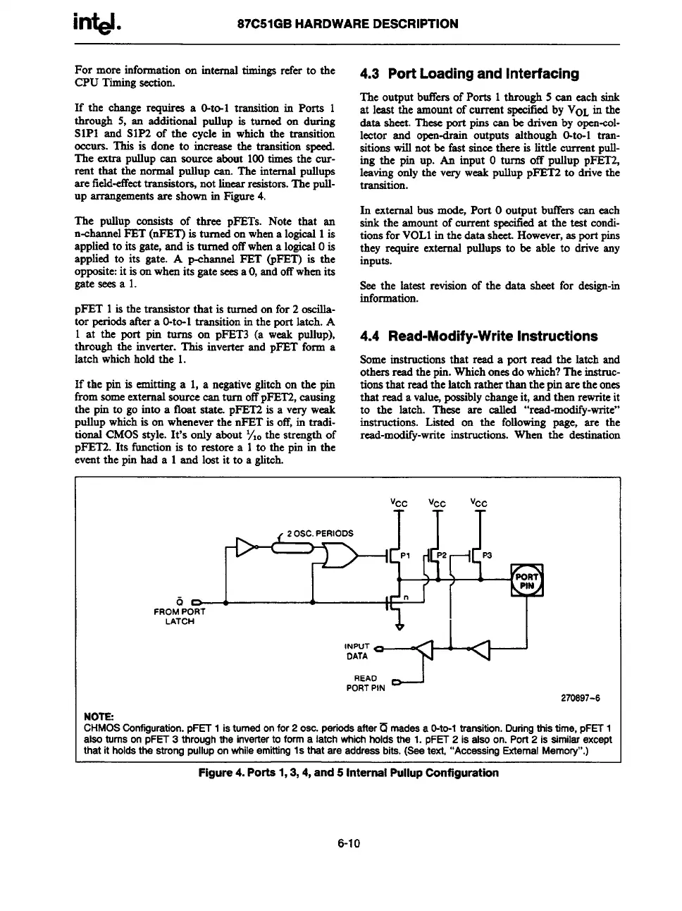
If the change requirea a o-t-l transition in Ports 1
through 5, an additional pullup is turned on during
SIPI and S1P2 of the cycle in whichthe transition
occurs. This is done to increase
the transition speed.
The extra pullup can source about 100times the cur-
rent that the normal pullup can. The internal pullups
are field-effecttransistors, not linearreaistors.Thepull-
UP
arrangementsare shownin Figure4.
The ptdlup consists of three pFETs. Note that an
n-channelF13T(nFET) is turnedon whena logical1is
appliedto its gate, and is turned offwhena logicalOis
applied to its gate. A p-channel FET @ET) is the
opposite:it isonwhenits gate seesa O,andoffwhenits
gate seesa 1.
pFET 1is the transistor that is turnedon for 2 oscilla-
tor periodsafter a O-to-1transitionin the port latch. A
1 at the port pin turns on pFET3 (a weak pullup),
through the inverter. This inverter and pFET form a
latch whichhold the 1.
If the pin is emitting a 1, a negativeglitch on the pin
fromsomeexternalsource can turn offpFET2,causing
the pin to go into a float state. pFET2is a very weak
pullupwhichis on wheneverthe nFET is off,in tradi-
tional CMOSstyle. It’s only about Ylothe strengthof
pFET2. Its functionis to restore a 1to the pin in the
eventthe pin had a 1 and lost it to a glitch.
4.3 Port Loading and Interfacing
TheoutputbuffersofPorts1through5 caneachsink
urrentspecitiedbyVoLinthe
atleasttheamountofc
dataSheet.TheseportPiIIScanbe
dliV~ by q)cn-col-
lector and open-drain outputs slthoug3 O-to-1tran-
sitionswillnot be fast sincethere is little
current pull-
ing the pin up. An input Oturns off pollup pFET2,
leavingonlythe very weakpulluppFET2 to drivethe
transition.
In external bns mode, Port Ooutput butkrs can each
sink the amount of current specitiedat the test condi-
tionsfor VOL1inthe data sheet.However,as port pins
they require external pullupsto be able to drive any
inputs.
See the latest revisionof the data sheet for design-in
information.
4.4 Read-Modify-Write Instructions
Someinstructionsthatreada portreadthelatchand
othersread the pin.Whichonesdowhich?Theinstruc-
tionsthat readthe latchrather than the
pinare theones
that read a VSJU?possiblychange
it,andthenrewriteit
to the latch. Theae are called “read-modify-write”
instructions. Listed on the following page, are the
read-modfjwrite instructions. When the destination
v~~
v~~
v~~
PI
Iil ~
P2
P3
,,
POUT
I’
PIN
6 D
n
FROMPORT
LATCH
INPUT
DATA
READ
PORTPIN
270897-6
NOTE:
CHMOSCotiiguration.pFET1isturnedonfor2OSC.periodsafterU msdesa O-to-1transition.Duringthistime,pFET1
alsoturnsonpFET3throughtheinvertertoforma latchwhkhholdsthe1.pFET2iaalsoon.Port2 issimilarexcept
thatitholdsthestrongpulluponwhileemittingIs thatare addressbits.(Seetext,“AcceaaingExternalMemory”.)
Figure4.Ports1,3,4, and5 internalPullupConfiguration
,
6-10