UM10360 All information provided in this document is subject to legal disclaimers. © NXP B.V. 2013. All rights reserved.
User manual Rev. 3 — 19 December 2013 37 of 841
NXP Semiconductors
UM10360
Chapter 4: LPC176x/5x Clocking and power control
4.5.2 PLL0 register description
PLL0 is controlled by the registers shown in Table 18. More detailed descriptions follow.
Warning: Improper setting of PLL0 values may result in incorrect operation of the
device!
[1] Reset Value reflects the data stored in used bits only. It does not include reserved bits content.
4.5.3 PLL0 Control register (PLL0CON - 0x400F C080)
The PLL0CON register contains the bits that enable and connect PLL0. Enabling PLL0
allows it to attempt to lock to the current settings of the multiplier and divider values.
Connecting PLL0 causes the processor and most chip functions to run from the PLL0
output clock. Changes to the PLL0CON register do not take effect until a correct PLL0
Table 18. PLL0 registers
Name Description Access Reset
value
[1]
Address
PLL0CON PLL0 Control Register. Holding register for
updating PLL0 control bits. Values written to this
register do not take effect until a valid PLL0 feed
sequence has taken place.
R/W 0 0x400F C080
PLL0CFG PLL0 Configuration Register. Holding register for
updating PLL0 configuration values. Values
written to this register do not take effect until a
valid PLL0 feed sequence has taken place.
R/W 0 0x400F C084
PLL0STAT PLL0 Status Register. Read-back register for
PLL0 control and configuration information. If
PLL0CON or PLL0CFG have been written to, but
a PLL0 feed sequence has not yet occurred, they
will not reflect the current PLL0 state. Reading
this register provides the actual values controlling
the PLL0, as well as the PLL0 status.
RO 0 0x400F C088
PLL0FEED PLL0 Feed Register. This register enables
loading of the PLL0 control and configuration
information from the PLL0CON and PLL0CFG
registers into the shadow registers that actually
affect PLL0 operation.
WO NA 0x400F C08C
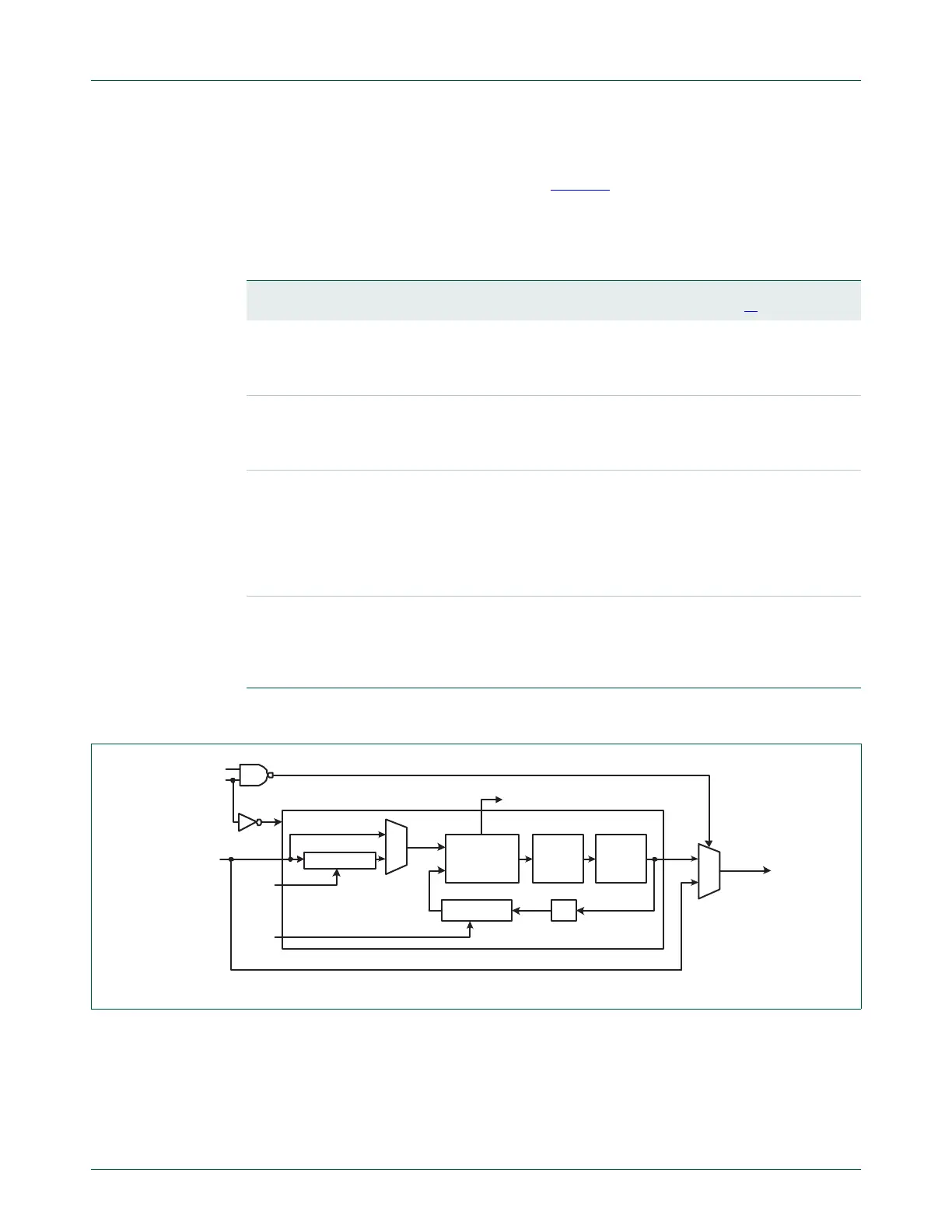
Fig 9. PLL0 block diagram
N-DIVIDER
M-DIVIDER
NSEL
[7:0]
PHASE-
FREQUENCY
DETECTOR
FILTER CCO
/2
MSEL
[14:0]
PLOCK
PLLE
PLLC
pd
refclk
pllclkin
pllclk

 Loading...


