Previous Page Table of Contents Section Contents
Back
Index Next Page
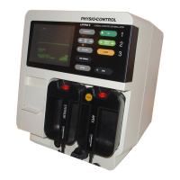
LIFEPAK 20/20e Defibrillator/Monitor Device Description
Functional Description (continued)
A01 System Control
PCB
The A01 System Control PCB provides the central control for the device. A
reduced instruction set computing (RISC) processor, along with a real-time clock
and digital memory, serve as the central processing unit (CPU). A companion
chip provides most of the discrete interfaces required within the device, including
the RS-232 and IrDA external communication ports. The data bus provides high-
speed communication between the A01 System Control PCB and other PCBs
within the device.
The major subsystems on the A01 System Control PCB are as follows:
■ Power Supplies — The A01 System Control PCB uses SW_VBatt
(switched battery voltage) from the A04 Therapy PCB to originate five power
supplies for use throughout the PCB as follows:
– ±5 V analog power for the analog ECG out, audio output circuitry, and
bus control
– +3.3 V logic power for the processor memory, companion chip and CPU
I/O
– +2.5 V logic power for the digital signal processor
– +2.0 V logic power for the CPU processor chip
– Patient-isolated ±10 and ±5 V analog power for the paddles pre-amp
3-21