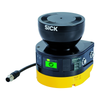
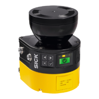
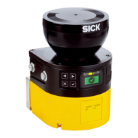
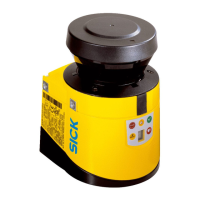
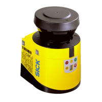
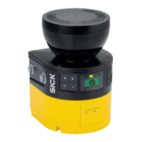
microScan3 Pro I/O
Test pulse width ≤ 300 µs (typ. 230 µs)
Test pulse interval
Scan cycle time 30 ms 240 ms … 264 ms (typ. 240 ms)
Scan cycle time 40 ms 320 ms to 344 ms (typ. 320 ms)
Scan cycle time 50 ms 400 ms
Duration of OFF state ≥ 80 ms
Discrepancy time (time
of
fset between switching
OSSDs of an OSSD pair)
≤ 1 ms (typ. 25 µs)
Universal output, universal I/O (configured as output)
Output voltage HIGH (U
V
– 2 V
) … U
V
Output voltage LOW 0 V … 2 V
Output current HIGH 0.5 mA ... 200 mA
3)
Leakage current ≤ 250 µA
Switch-on delay time
5)
40 ms
Switch off delay
6)
40 ms
Static control input, universal input, universal I/O (configured as input)
Input voltage HIGH 24 V (11 V ... 30 V)
Input voltage LOW 0 V (–30 V … 5 V)
Input current HIGH 2 mA ... 3 mA
Input current LOW 0 mA … 2 mA
Input capacitance 10 nF
Input frequency (max.
s
witching sequence when
used as control input)
≤ 20 Hz
Sampling time 4 ms
Response time at EDM after
s
witching on OSSDs (when
used as EDM input)
300 ms
Actuating duration of control
switch for reset (when used
as reset input)
60 ms to 30 s
Actuating duration of switch
for sleep mode (when used
as sleep mode input)
≥ 120 ms
Dynamic control input
Input voltage HIGH 24 V (11 V ... 30 V)
Input voltage LOW 0 V (-30 V ... 5 V)
Input current HIGH 2 mA ... 3 mA
Input current LOW 0 mA ... 2 mA
Input capacitance Typ. 2 nF
Input frequency < 100 kHz
Duty cycle (Ti/T) 0.5
Voltage supply for incremental encoders
Voltage output (U
V
– 1 V
) … U
V
Current load ≤ 100 mA
7)
TECHNICAL DATA 13
8025424/1ELL/2022-01-21 | SICK O P E R A T I N G I N S T R U C T I O N S | microScan3 Pro I/O
183
Subject to change without notice