Embedded Flash memory (FLASH) RM0453
100/1454 RM0453 Rev 2
memory clock (HCLK3) and the internal voltage range of the device (V
CORE
). Refer to
Section 6.1.4: Dynamic voltage scaling management.
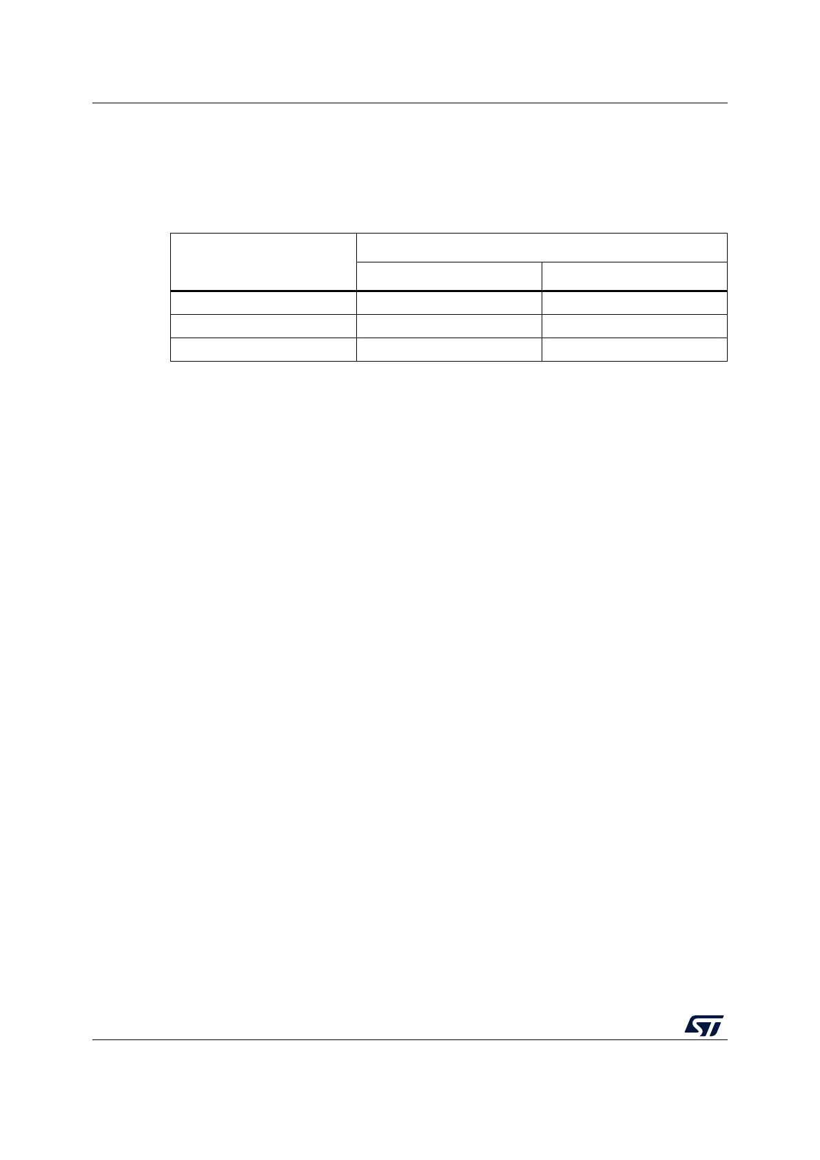
The table below shows the correspondence between wait states and frequency of the Flash
memory clock.
After power-on reset and wakeup from Standby, the HCLK3 clock frequency is 4 MHz in
range 1 and 0 wait state (WS) is configured in FLASH_ACR.
When changing the frequency of the Flash memory clock or the V
CORE
range, the software
sequences detailed below must be applied in order to tune the number of wait states
needed to access the Flash memory:
Increase the CPU frequency
1. Program the new number of wait states to the LATENCY[2:0] bits in FLASH_ACR.
2. Check that the new number of wait states is taken into account to access the Flash
memory by reading back the LATENCY[2:0] bits in FLASH_ACR, and wait until the new
programmed number is read.
3. Modify the system cock source by writing the SW[1:0] bits in RCC_CFGR.
4. If needed, modify the CPU clock prescaler by writing the SHDHPRE[3:0] bits in
RCC_EXTCFGR.
5. Optionally, check that the new system clock source or/and the new Flash memory clock
prescaler value is/are taken into account by reading the clock source status (SWS(1:0]
bits) in RCC_CFGR, or/and the AHB prescaler value (SHDHPREF bit) in
RCC_EXTCFGR.
Decrease the CPU frequency
1. Modify the system clock source by writing the SW[1:0] bits in RCC_CFGR.
2. If needed, modify the Flash memory clock prescaler by writing the SHDHPRE[3:0] bits
in RCC_EXTCFGR.
3. Check that the new system clock source or/and the new Flash memory clock prescaler
value is/are taken into account by reading the clock source status (SWS[1:0] bits) in
RCC_CFGR, or/and the AHB prescaler value (SHDHPREF bit) in RCC_EXTCFGR.
Wait until the new programmed system clock source or/and new Flash memory clock
prescaler value is/are read.
4. Program the new number of wait states to the LATENCY[2:0] bits in FLASH_ACR.
5. Optionally, check that the new number of wait states is used to access the Flash
memory by reading back the LATENCY[2:0] bits in FLASH_ACR.
Table 12. Number of wait states according to Flash clock (HCLK3) frequency
Wait states (WS)
(access)
HCLK3 (MHz)
V
CORE
range 1 V
CORE
range 2
0 WS (1 HCLK cycle) ≤ 18 ≤ 6
1 WS (2 HCLK cycles) ≤ 36 ≤ 12
2 WS (3 HCLK cycles) ≤ 48 ≤ 16

 Loading...


