AES hardware accelerator (AES) RM0453
682/1454 RM0453 Rev 2
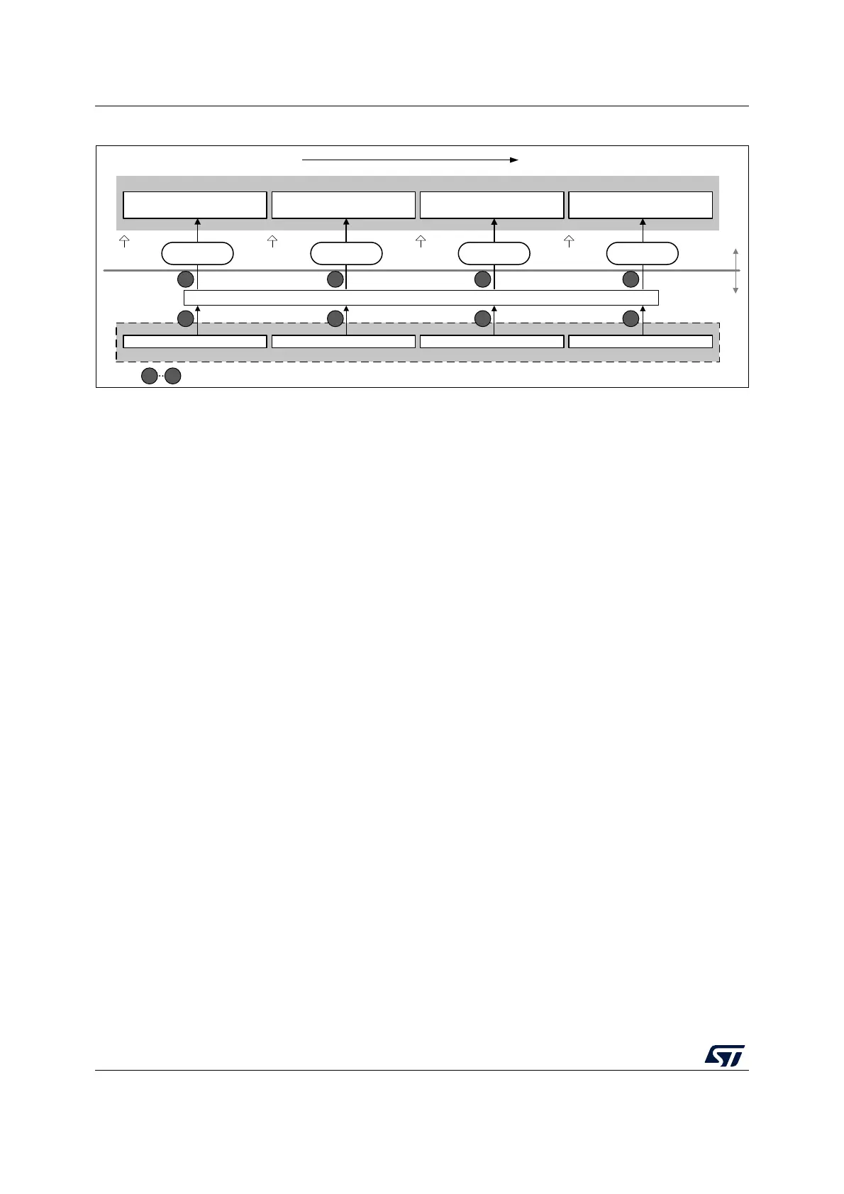
Figure 126. DMA transfer of a 128-bit data block during output phase
DMA operation in different operating modes
DMA operations are usable when Mode 1 (encryption) or Mode 3 (decryption) are selected
via the MODE[1:0] bitfield of the register AES_CR. As in Mode 2 (key derivation) the
AES_KEYRx registers must be written by software, enabling the DMA transfer through the
DMAINEN and DMAOUTEN bits of the AES_CR register have no effect in that mode.
DMA single requests are generated by AES until it is disabled. So, after the data output
phase at the end of processing of a 128-bit data block, AES switches automatically to a new
data input phase for the next data block, if any.
When the data transferring between AES and memory is managed by DMA, the CCF flag is
not relevant and can be ignored (left set) by software. It must only be cleared when
transiting back to data transferring managed by software. See Suspend/resume operations
in ECB/CBC modes in Section 23.4.8: AES basic chaining modes (ECB, CBC) as example.
23.4.17 AES error management
AES configuration can be changed at any moment by clearing the EN bit of the AES_CR
register.
Read error flag (RDERR)
Unexpected read attempt of the AES_DOUTR register sets the RDERR flag of the AES_SR
register, and returns zero.
RDERR is triggered during the computation phase or during the input phase.
Note: AES is not disabled upon a RDERR error detection and continues processing.
An interrupt is generated if the ERRIE bit of the AES_CR register is set. For more details,
refer to Section 23.5: AES interrupts.
The RDERR flag is cleared by setting the ERRIE bit of the AES_CR register.
Write error flag (WDERR)
Unexpected write attempt of the AES_DINR register sets the WRERR flag of the AES_SR
register, and has no effect on the AES_DINR register. The WRERR is triggered during the
computation phase or during the output phase.
MSv42161V1
AES core output buffer
LSB
MSB
(No swapping)
Memory accessed through DMA
Word2Word3 Word0Word1
DMA
single read
DMA req N DMA req N+1 DMA req N+2 DMA req N+3
O127 O96
O63 O32
O31 O0
O64O95
D127 D96
D63 D32
D31 D0
D64D95
DOUT[127:96] DOUT[95:64] DOUT[63:32] DOUT[31:0]
DMA
single read
DMA
single read
DMA
single read
Chronological order
Increasing address
LSBMSB
System
AES
peripheral
1 2 3 4
1 2 3 4
1
Order of read from AES_DOUTR
4
AES_DOUTR

 Loading...


