Debug support (DBG) RM0453
1420/1454 RM0453 Rev 2
Refer to Section 38.12: Microcontroller debug unit (DBGMCU) for the register boundary
addresses.
38.13 CPU2 ROM tables
The ROM tables are CoreSight components that contain the base addresses of all the
CoreSight debug components accessible via the AHBD. These tables allow a debugger to
discover the topology of the CoreSight system automatically.
There are two ROM tables in the CPU2 sub-system:
• ROM1: CPU2 processor ROM table, pointed to by the AP_BASER register in the CPU2
AHB-AP. It contains the base address pointers for the CTI, as well as for the CPU2
ROM table.
• ROM2: CPU2 ROM table, containing pointers to the CPU2 system control space (SCS)
registers, which allow the debugger to identify the CPU core, as well as the remaining
CoreSight components in the CPU2 subsystem (PBU, DWT).
ROM1 occupies a 4-Kbyte, 32-bit wide chunk of AHB address space, from 0xF0000000 to
0xF0000FFC.
0x048
DBGMCU_
C2APB1FZR2
Res.
Res.
Res.
Res.
Res.
Res.
Res.
Res.
Res.
Res.
Res.
Res.
Res.
Res.
Res.
Res.
Res.
Res.
Res.
Res.
Res.
Res.
Res.
Res.
Res.
DBG_LPTIM3_STOP
DBG_LPTIM2_STOP
Res.
Res.
Res.
Res.
Res.
Reset value 00
0x04C
DBGMCU_
APB2FZR
Res.
Res.
Res.
Res.
Res.
Res.
Res.
Res.
Res.
Res.
Res.
Res.
Res.
DBG_TIM17_STOP
DBG_TIM16_STOP
Res.
Res.
Res.
Res.
Res.
DBG_TIM1_STOP
Res.
Res.
Res.
Res.
Res.
Res.
Res.
Res.
Res.
Res.
Res.
Reset value 0 0 0
0x050
DBGMCU_
C2APB2FZR
Res.
Res.
Res.
Res.
Res.
Res.
Res.
Res.
Res.
Res.
Res.
Res.
Res.
DBG_TIM17_STOP
DBG_TIM16_STOP
Res.
Res.
Res.
Res.
Res.
DBG_TIM1_STOP
Res.
Res.
Res.
Res.
Res.
Res.
Res.
Res.
Res.
Res.
Res.
Reset value 0 0 0
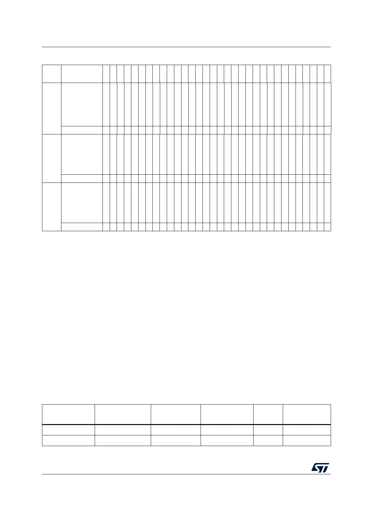
Table 282. DBGMCU register map and reset values (continued)
Offset Register name
31
30
29
28
27
26
25
24
23
22
21
20
19
18
17
16
15
14
13
12
11
10
9
8
7
6
5
4
3
2
1
0
Table 283. ROM1 table
Address in ROM
table
Component name
Component base
address
Component
address offset
Size Entry
0xF0000000 CPU2 ROM table 0xE00FF000 0xF00FF000 4 KB 0xF00FF003
0xF0000004 CTI 0xF0001000 0x00001000 4 KB 0x00001003

 Loading...


