RM0453 Rev 2 113/1454
RM0453 Embedded Flash memory (FLASH)
153
4.4.2 Option bytes programming
After a reset, the options related bits in FLASH_CR and FLASH_C2CR are write-protected.
To run any operation on the option bytes page, the option lock bit OPTLOCK in FLASH_CR
must be cleared.
The following sequence is used to unlock the FLASH_CR and Flash memory option
registers:
1. Unlock FLASH_CR with the LOCK clearing sequence (refer to Unlocking the Flash
memory).
2. Write OPTKEY1 = 0x0819 2A3B in FLASH_OPTKEYR
3. Write OPTKEY2 = 0x4C5D 6E7F in FLASH_OPTKEYR
Any wrong sequence locks up the Flash option register until the next system reset. In the
case of a wrong key sequence, a bus error is detected and a hard fault interrupt is
generated.
The user options can be protected against unwanted erase/program operations by setting
the OPTLOCK bit by software.
Note: If LOCK is set by software, OPTLOCK is automatically set as well.
Note: In a multi-CPU system, it is good practice to use semaphores to manage option
programming and prevent simultaneous option programming by the CPUs.
Modify user options
The option bytes are programmed differently from a main memory user address.
To modify the user options value, follow the procedure below:
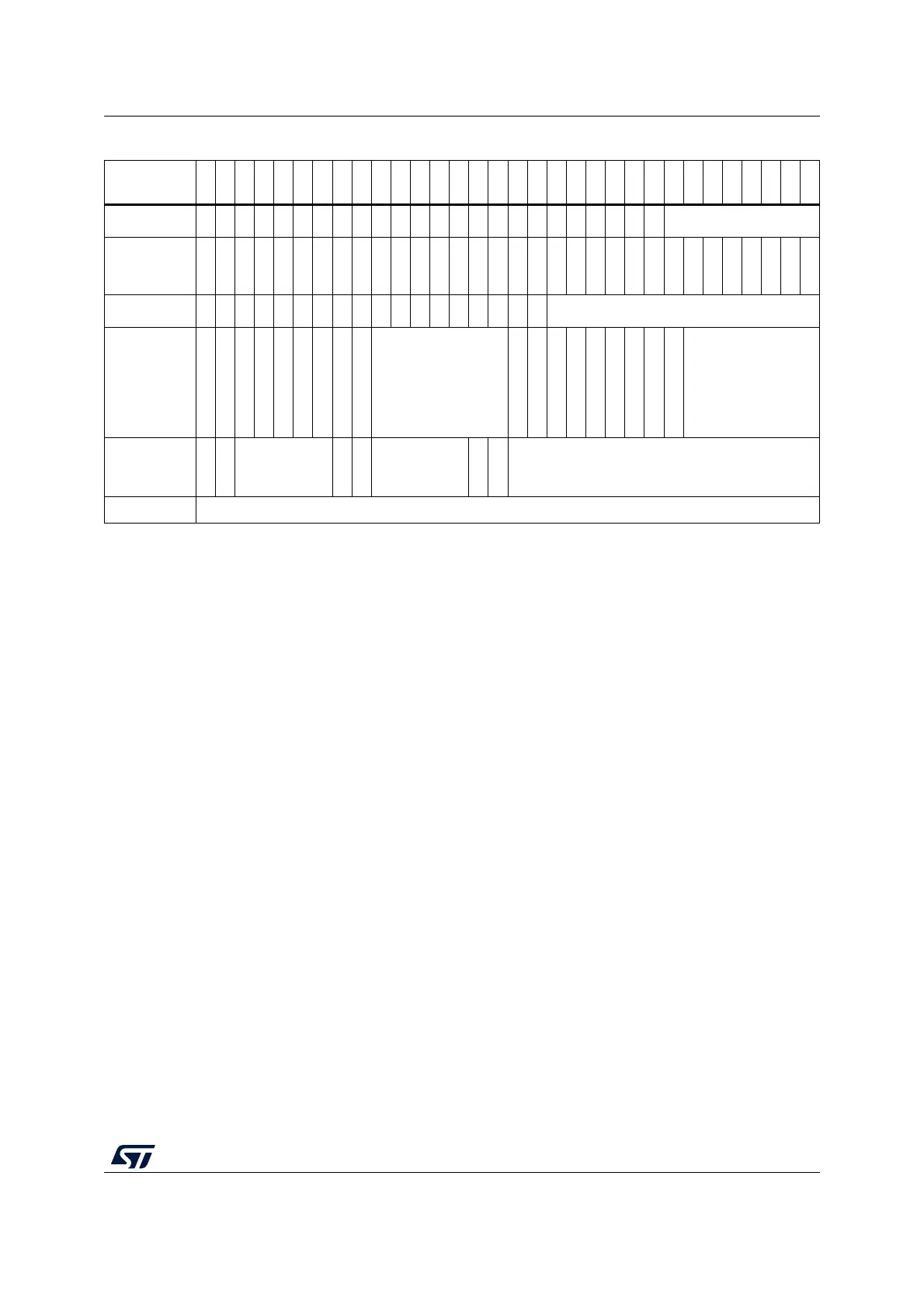
0x1FFF 7830
Res.
Res.
Res.
Res.
Res.
Res.
Res.
Res.
Res.
Res.
Res.
Res.
Res.
Res.
Res.
Res.
Res.
Res.
Res.
Res.
Res.
Res.
Res.
Res.
PCROP1B_END[7:0]
0x1FFF 7838
to
0x1FFF 7860
Res.
Res.
Res.
Res.
Res.
Res.
Res.
Res.
Res.
Res.
Res.
Res.
Res.
Res.
Res.
Res.
Res.
Res.
Res.
Res.
Res.
Res.
Res.
Res.
Res.
Res.
Res.
Res.
Res.
Res.
Res.
Res.
0x1FFF 7868
Res.
Res.
Res.
Res.
Res.
Res.
Res.
Res.
Res.
Res.
Res.
Res.
Res.
Res.
Res.
Res.
Res.
Res.
IPCCDBA[13:0]
0x1FFF 7870
SUBGHZSPISD
Res.
Res.
Res.
Res.
Res.
Res.
Res.
HDPAD
HDPSA[6:0]
Res.
Res.
Res.
DDS
Res.
Res.
Res.
Res.
FSD
SFSA[6:0]
0x1FFF 7878
C2OPT
NBRSD
SNBRSA[4:0]
Res.
BRSD
SBRSA[4:0]
Res.
Res.
SBRV[15:0]
0x1FFF 7FF8
OPTVAL[31:0]
1. The upper 32 bits of the double-word address contain the inverted data from the lower 32 bits.
Table 16. Option bytes organization (continued)
Address
(1)
31
30
29
28
27
26
25
24
23
22
21
20
19
18
17
16
15
14
13
12
11
10
9
8
7
6
5
4
3
2
1
0

 Loading...


