Debug support (DBG) RM0453
1340/1454 RM0453 Rev 2
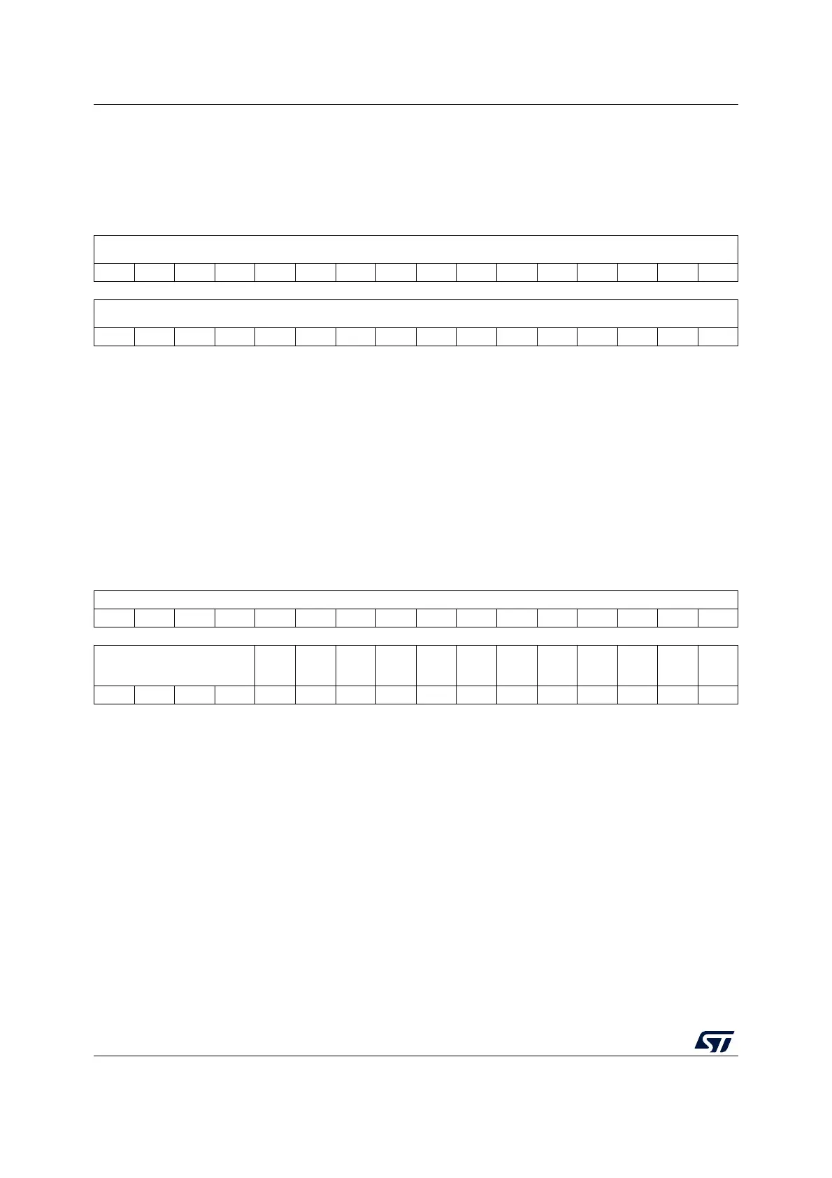
38.5.4 AP banked data registers x (AP_BDxR)
Address offset: 0x10 + 0x04 * x, (x=0 to 3)
Reset value: 0x0000 0000
38.5.5 AP base address register (AP_BASER)
Address offset: 0xF8
Reset value: 0xE00F F003 (AP0)
Reset value: 0xF000 0003 (AP1)
31 30 29 28 27 26 25 24 23 22 21 20 19 18 17 16
TBD[31:16]
rw rw rw rw rw rw rw rw rw rw rw rw rw rw rw rw
1514131211109876543210
TBD[15:0]
rw rw rw rw rw rw rw rw rw rw rw rw rw rw rw rw
Bits 31:0 TBD[31:0]: banked data of current transfer to address AP_TAR.TA
TA + AP_BDnR address [3:2] + 0b00
Auto address incrementing is not performed on AP_BD[3:0]R.
Banked transfers are only supported for word transfers.
31 30 29 28 27 26 25 24 23 22 21 20 19 18 17 16
BASEADDR[19:4]
rrrrrrrrrrrrrrrr
1514131211109876543210
BASEADDR[3:0] Res. Res. Res. Res. Res. Res. Res. Res. Res. Res.
FORM
AT
ENTRY
PRESE
NT
rrrr rr
Bits 31:12 BASEADDR[19:0]: base address (bits 31 to 12) of ROM table for the AP
The 12 LSBs are zero since the ROM table must be aligned on a 4-Kbyte boundary.
AP0 CPU1 (Cortex-M4) AHB-AP: 0xE00FF
AP1 CPU2 (Cortex-M0+) AHB-AP: 0xF0000
Bits 11:2 Reserved, must be kept at reset value.
Bit 1 FORMAT: base address register format
1: Arm debug interface v5
Bit 0 ENTRYPRESENT: Indicates that debug components are present on the access port bus.
1: Debug components are present

 Loading...


