Digital-to-analog converter (DAC) RM0453
594/1454 RM0453 Rev 2
19.4.2 DAC pins and internal signals
The DAC includes:
• One output channel
• The DACx_OUT1 can be disconnected from the output pin and used as an ordinary
GPIO
• The dac_out1 can use an internal pin connection to on-chip peripherals such as
comparator, operational amplifier and ADC (if available).
• DAC output channel buffered or non buffered
• Sample and hold block and registers operational in Stop mode, using the LSI clock
source (dac_hold_ck) for static conversion.
The DAC includes up to two separate output channels. Each output channel can be
connected to on-chip peripherals such as comparator, operational amplifier and ADC (if
available). In this case, the DAC output channel can be disconnected from the DACx_OUT1
output pin and the corresponding GPIO can be used for another purpose.
The DAC output can be buffered or not. The Sample and hold block and its associated
registers can run in Stop mode using the LSI clock source (dac_hold_ck).
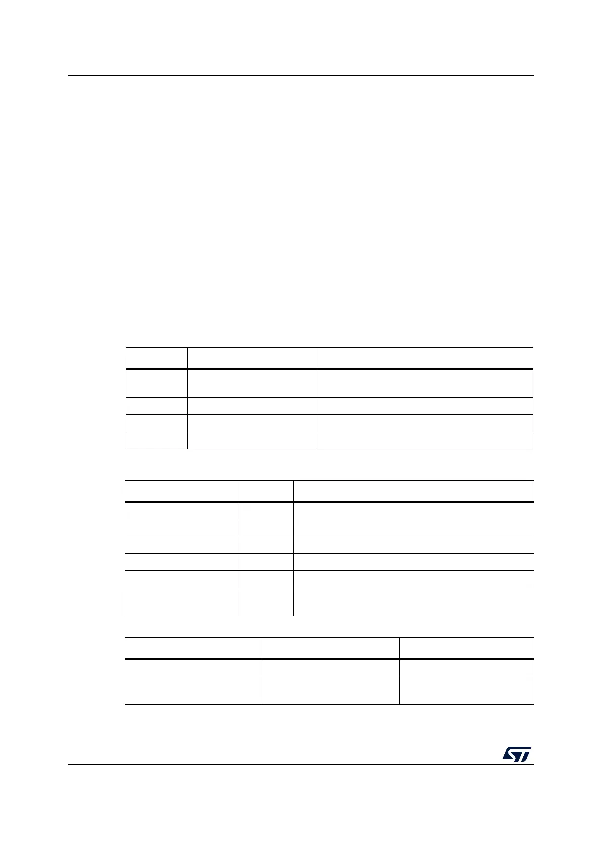
Table 112. DAC input/output pins
Pin name Signal type Remarks
VREF+
Input, analog reference
positive
The higher/positive reference voltage for the DAC,
V
REF+
≤ V
DDAmax
(refer to datasheet)
VDD Input, analog supply Analog power supply
VSS Input, analog supply ground Ground for analog power supply
DACx_OUT1 Analog output signal DACx channel1 analog output
Table 113. DAC internal input/output signals
Internal signal name Signal type Description
dac_ch1_dma Bidirectional DAC channel1 DMA request/acknowledge
dac_ch1_trgx (x = 1 to 15) Inputs DAC channel1 trigger inputs/acknowledge
dac_unr_it Output DAC underrun interrupt
dac_pclk Input DAC peripheral clock
dac_hold_ck Input DAC low-power clock used in Sample and hold mode
dac_out1
Analog
output
DAC channel1 output for on-chip peripherals
Table 114. DAC interconnection
Signal name Source Source type
dac_hold_ck ck_lsi LSI clock selected in the RCC
dac_ch1_trg1 tim1_trgo
Internal signal from on-chip
timers TIM1_TGO_CKTIM

 Loading...


