Digital-to-analog converter (DAC) RM0453
602/1454 RM0453 Rev 2
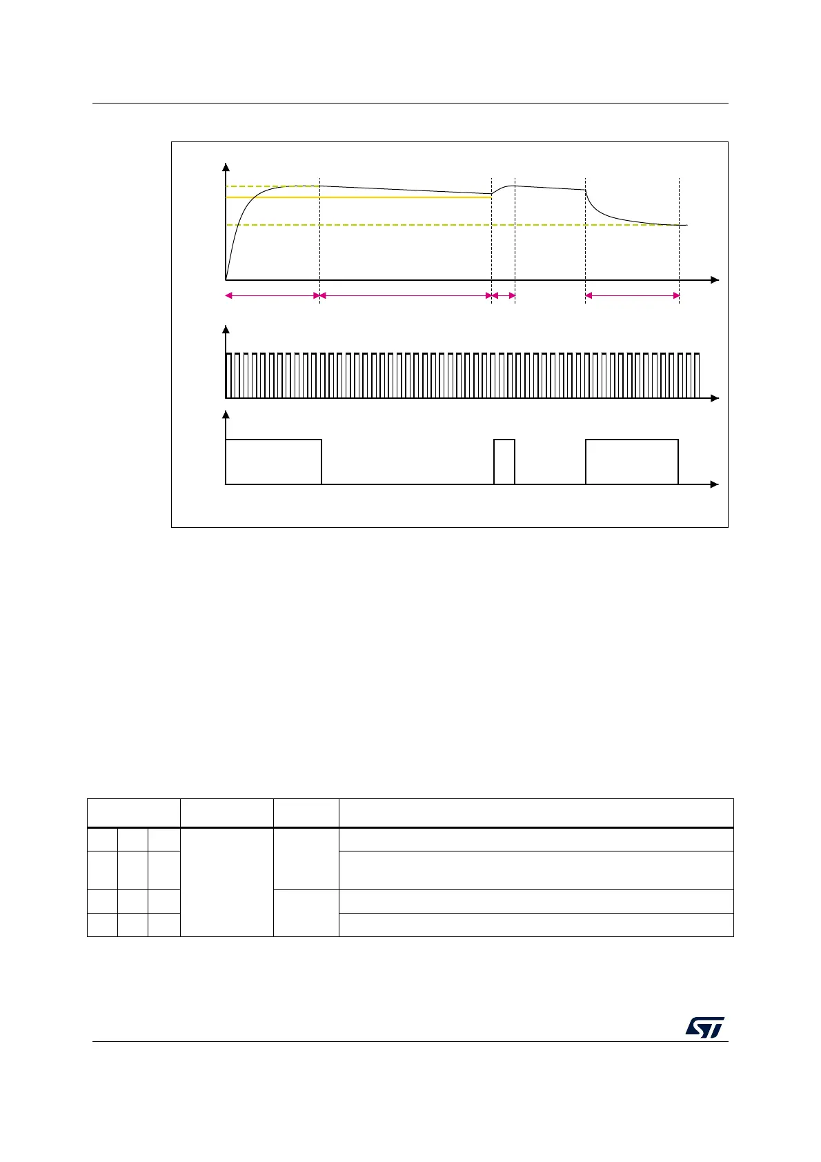
Figure 93. DAC Sample and hold mode phase diagram
Like in Normal mode, the Sample and hold mode has different configurations.
To enable the output buffer, MODE1[2:0] bits in DAC_MCR register must be set to:
• 100: DAC is connected to the external pin
• 101: DAC is connected to external pin and to on chip peripherals
To disabled the output buffer, MODE1[2:0] bits in DAC_MCR register must be set to:
• 110: DAC is connected to external pin and to on chip peripherals
• 111: DAC is connected to on chip peripherals
When MODE1[2:0] bits are equal to 111, an internal capacitor, C
Lint
, holds the voltage
output of the DAC core and then drive it to on-chip peripherals.
All Sample and hold phases are interruptible, and any change in DAC_DHR1 immediately
triggers a new sample phase.
MSv45340V3
dac_hold
_ck
DAC
ON ONON
t
t
V
1
V
2
Sampling phase Hold phase
Refresh
phase
Sampling phase
V
d
Table 116. Channel output modes summary
MODE1[2:0] Mode Buffer Output connections
000
Normal mode
Enabled
Connected to external pin
001
Connected to external pin and to on chip-peripherals (such as
comparators)
010
Disabled
Connected to external pin
0 1 1 Connected to on chip peripherals (such as comparators)

 Loading...


