RM0453 Rev 2 601/1454
RM0453 Digital-to-analog converter (DAC)
617
The timings for the three phases above are in units of LSI clock periods. As an example, to
configure a sample time of 350 µs, a hold time of 2 ms and a refresh time of 100 µs
assuming LSI ~32 KHz is selected:
12 cycles are required for sample phase: TSAMPLE1[9:0] = 11,
62 cycles are required for hold phase: THOLD1[9:0] = 62,
and 4 cycles are required for refresh period: TREFRESH1[7:0] = 4.
In this example, the power consumption is reduced by almost a factor of 15 versus Normal
modes.
The formulas to compute the right sample and refresh timings are described in the table
below, the Hold time depends on the leakage current.
Example of the sample and refresh time calculation with output buffer on
The values used in the example below are provided as indication only. Please refer to the
product datasheet for product data.
C
SH
= 100 nF
V
DD
= 3.0 V
Sampling phase:
t
SAMP
= 7 μs + (10 * 2000 * 100 * 10
-9
) = 2.007 ms
(where R
BON
= 2 kΩ)
Refresh phase:
t
REFRESH
= 7 μs + (2000 * 100 * 10
-9
) * ln(2*10) = 606.1 μs
(where N
LSB
= 10 (10 LSB drop during the hold phase)
Hold phase:
D
v
= i
leak
* t
hold
/ C
SH
= 0.0073 V (10 LSB of 12bit at 3 V)
i
leak
= 150 nA (worst case on the IO leakage on all the temperature range)
t
hold
= 0.0073 * 100 * 10
-9
/ (150 * 10
-9
) = 4.867 ms
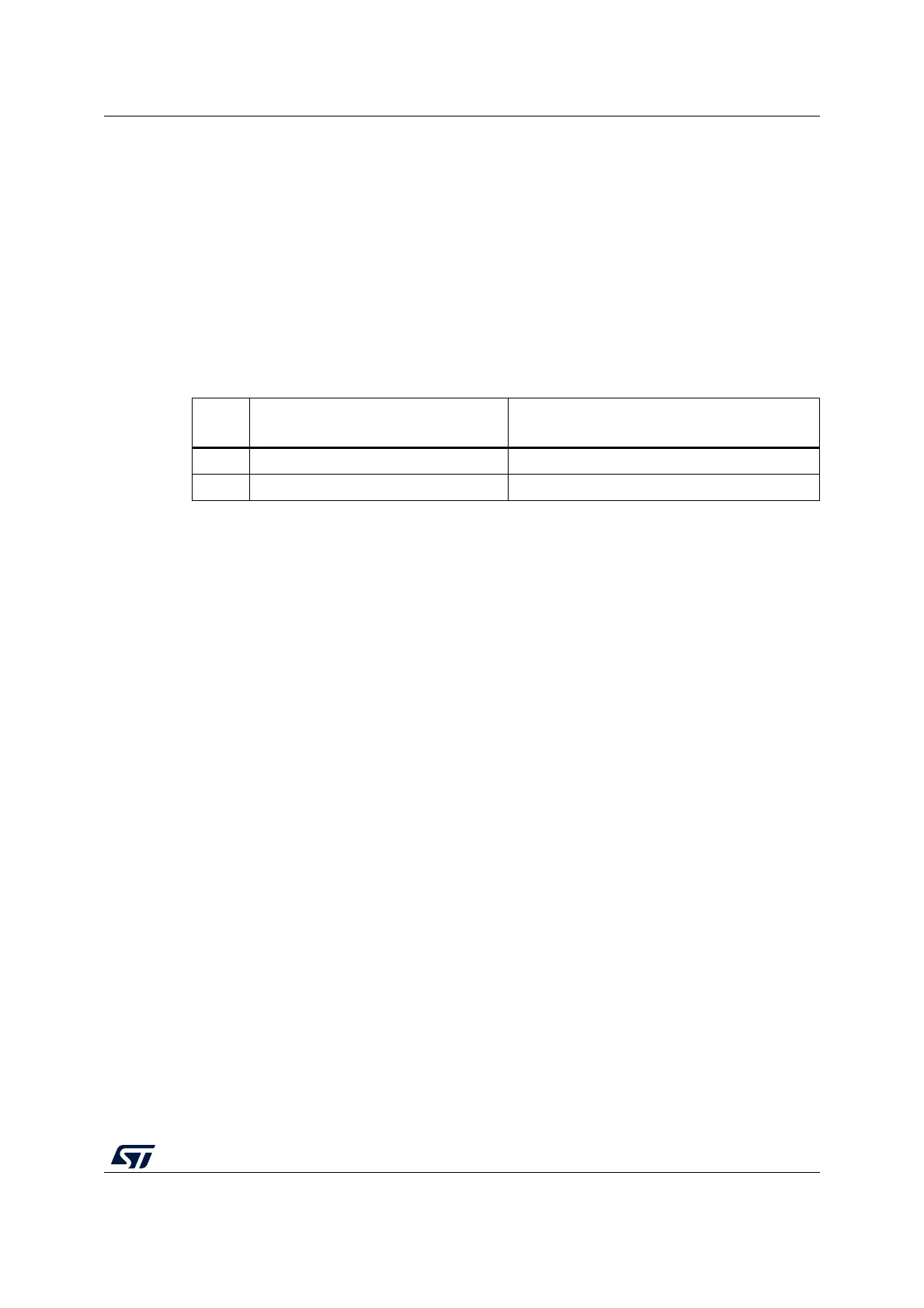
Table 115. Sample and refresh timings
Buffer
State
t
SAMP
(1)(2)
1. In the above formula the settling to the desired code value with ½ LSB or accuracy requires 10 constant
time for 12 bits resolution. For 8 bits resolution, the settling time is 7 constant time.
2. C
SH
is the capacitor in Sample and hold mode.
t
REFRESH
(2)(3)
3. The tolerated voltage drop during the hold phase “Vd” is represented by the number of LSBs after the
capacitor discharging with the output leakage current. The settling back to the desired value with ½ LSB
error accuracy requires ln(2*Nlsb) constant time of the DAC.
Enable 7 μs + (10*R
BON
*C
SH
)7 μs + (R
BON
*C
SH
)*ln(2*N
LSB
)
Disable 3 μs + (10*R
BOFF
*C
SH
)3 μs + (R
BOFF
*C
SH
)*ln(2*N
LSB
)

 Loading...


