Reset and clock control (RCC) RM0453
318/1454 RM0453 Rev 2
7.4.16 RCC AHB2 peripheral clock enable register (RCC_AHB2ENR)
Address offset: 0x04C
Reset value: 0x0000 0000
Access: no wait state, word, half-word and byte access
Note: When the peripheral clock is not active, the peripheral registers read or write access from
CPU1 is not supported.
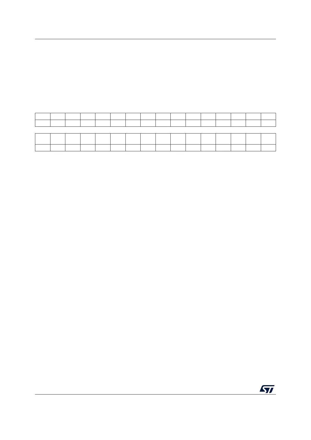
31 30 29 28 27 26 25 24 23 22 21 20 19 18 17 16
Res. Res. Res. Res. Res. Res. Res. Res. Res. Res. Res. Res. Res. Res. Res. Res.
1514131211109876543210
Res. Res. Res. Res. Res. Res. Res. Res.
GPIOH
EN
Res. Res. Res. Res.
GPIOC
EN
GPIOB
EN
GPIOA
EN
rw rw rw rw
Bits 31:8 Reserved, must be kept at reset value.
Bit 7 GPIOHEN: CPU1 IO port H clock enable
This bit is set and cleared by software.
0: IO port H clock disabled for CPU1
1: IO port H clock enabled for CPU1
Bits 6:3 Reserved, must be kept at reset value.
Bit 2 GPIOCEN: CPU1 IO port C clock enable
This bit is set and cleared by software.
0: IO port C clock disabled for CPU1
1: IO port C clock enabled for CPU1
Bit 1 GPIOBEN: CPU1 IO port B clock enable
This bit is set and cleared by software.
0: IO port B clock disabled for CPU1
1: IO port B clock enabled for CPU1
Bit 0 GPIOAEN: CPU1 IO port A clock enable
This bit is set and cleared by software.
0: IO port A clock disabled for CPU1
1: IO port A clock enabled for CPU1

 Loading...


