RM0453 Rev 2 583/1454
RM0453 Analog-to-digital converter (ADC)
591
18.12.9 ADC channel selection register [alternate] (ADC_CHSELR)
Address offset: 0x28
Reset value: 0x0000 0000
The same register can be used in two different modes:
– Each ADC_CHSELR bit enables an input (CHSELRMOD = 0 in ADC_CFGR1). Refer to
the current section.
– ADC_CHSELR is able to sequence up to 8 channels (CHSELRMOD = 1 in
ADC_CFGR1). Refer to next section.
CHSELRMOD = 0 in ADC_CFGR1
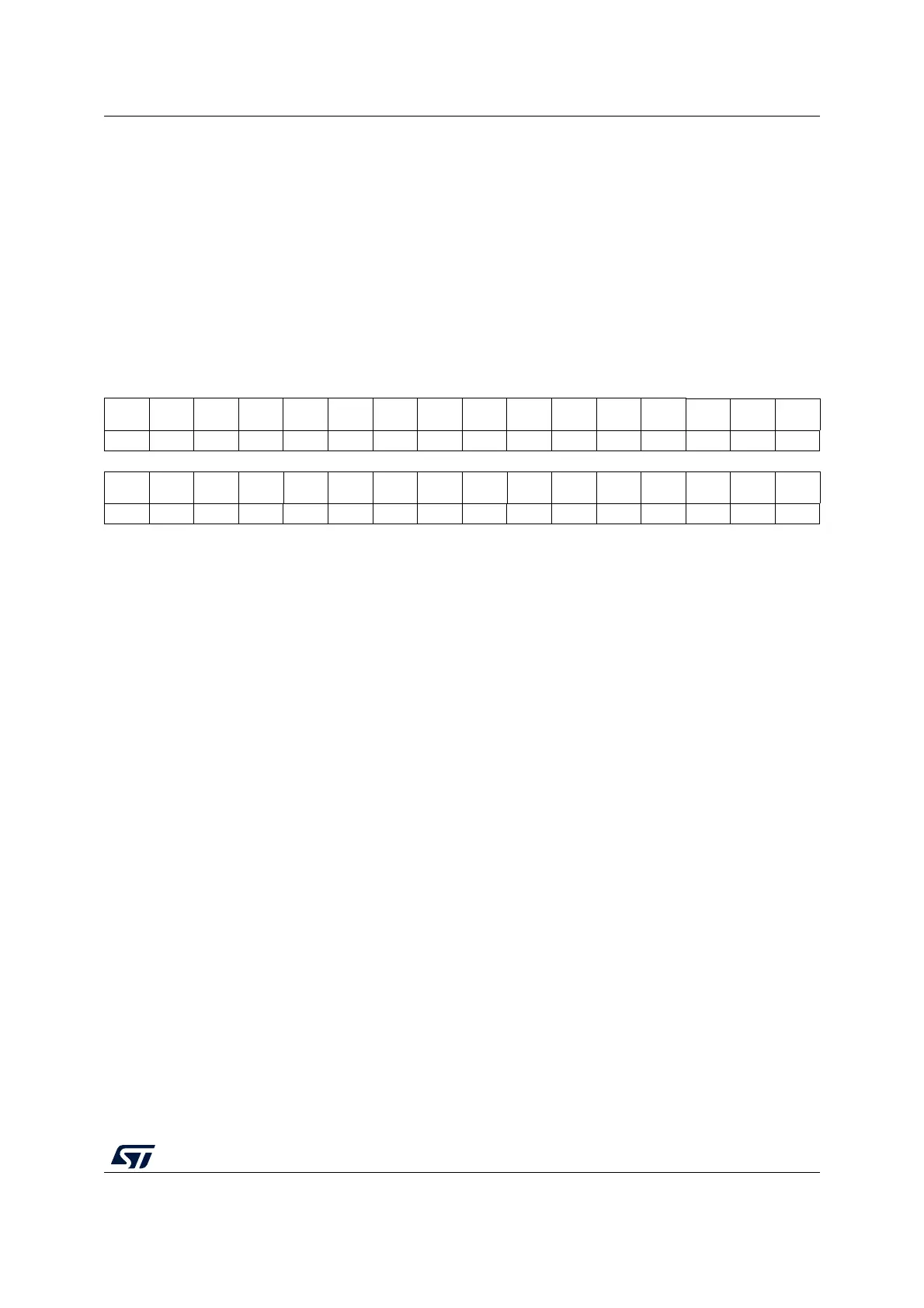
31 30 29 28 27 26 25 24 23 22 21 20 19 18 17 16
Res. Res. Res. Res. Res. Res. Res. Res. Res. Res. Res. Res. Res. Res.
CHSEL
17
CHSEL
16
rw rw
1514131211109876543210
CHSEL
15
CHSEL
14
CHSEL
13
CHSEL
12
CHSEL
11
CHSEL
10
CHSEL
9
CHSEL
8
CHSEL
7
CHSEL
6
CHSEL
5
CHSEL
4
CHSEL
3
CHSEL
2
CHSEL
1
CHSEL
0
rw rw rw rw rw rw rw rw rw rw rw rw rw rw rw rw
Bits 31:18 Reserved, must be kept at reset value.
Bits 17:0 CHSEL[17:0]: Channel-x selection
These bits are written by software and define which channels are part of the sequence of channels
to be converted. Refer to Figure 63: ADC connectivity for ADC inputs connected to external
channels and internal sources.
0: Input Channel-x is not selected for conversion
1: Input Channel-x is selected for conversion
Note: The software is allowed to write this bit only when ADSTART = 0 (which ensures that no
conversion is ongoing).
If CCRDY is not yet asserted after channel configuration (writing ADC_CHSELR register or
changing CHSELRMOD or SCANDIR), the value written to this bit is ignored.

 Loading...


