144 www.xilinx.com 7 Series FPGAs SelectIO Resources User Guide
UG471 (v1.10) May 8, 2018
Chapter 3: Advanced SelectIO Logic Resources
ISERDESE2 contains dedicated circuitry (including the OCLK input pin) to handle the
strobe-to-FPGA clock domain crossover entirely within the ISERDESE2 block. This
allows for higher performance and a simplified implementation.
• Dedicated support for networking interfaces
• Dedicated support for DDR3 interfaces
• Dedicated support for QDR interfaces
• Dedicated support for asynchronous interfaces
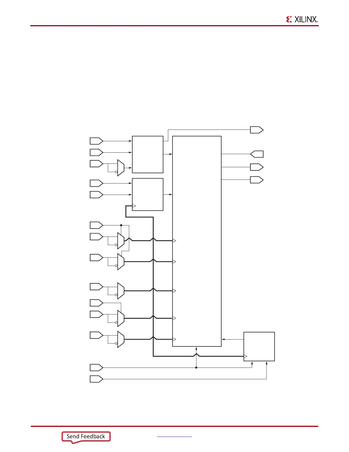
Figure 3-1 shows the block diagram of the ISERDESE2, highlighting all the major
components and features of the block including the optional inverters.
X-Ref Target - Figure 3-1
Figure 3-1: ISERDESE2 Block Diagram
UG471_c3_01_080210
OFB
O
IOB
Multiplexers
DDLY
SHIFTIN1/2
SHIFTOUT1/2
Q1:Q8
CE1
CE
Module
Serial-to-
Parallel
Converter
Bitslip
Module
CE2
RST
BITSLIP
D
DYNCLKSEL
CLKB
CLK
DYNCLKDIVSEL
CLKDIV
CLKDIVP
OCLK
 Loading...

