7 Series FPGAs SelectIO Resources User Guide www.xilinx.com 93
UG471 (v1.10) May 8, 2018
Supported I/O Standards and Terminations
• The differential signals at the input pins meet the V
IDIFF
(min) requirements in the
corresponding LVDS or LVDS_25 DC specifications tables of the specific device family
data sheet.
• For HR I/O banks in bidirectional configuration, internal differential termination is
always used.
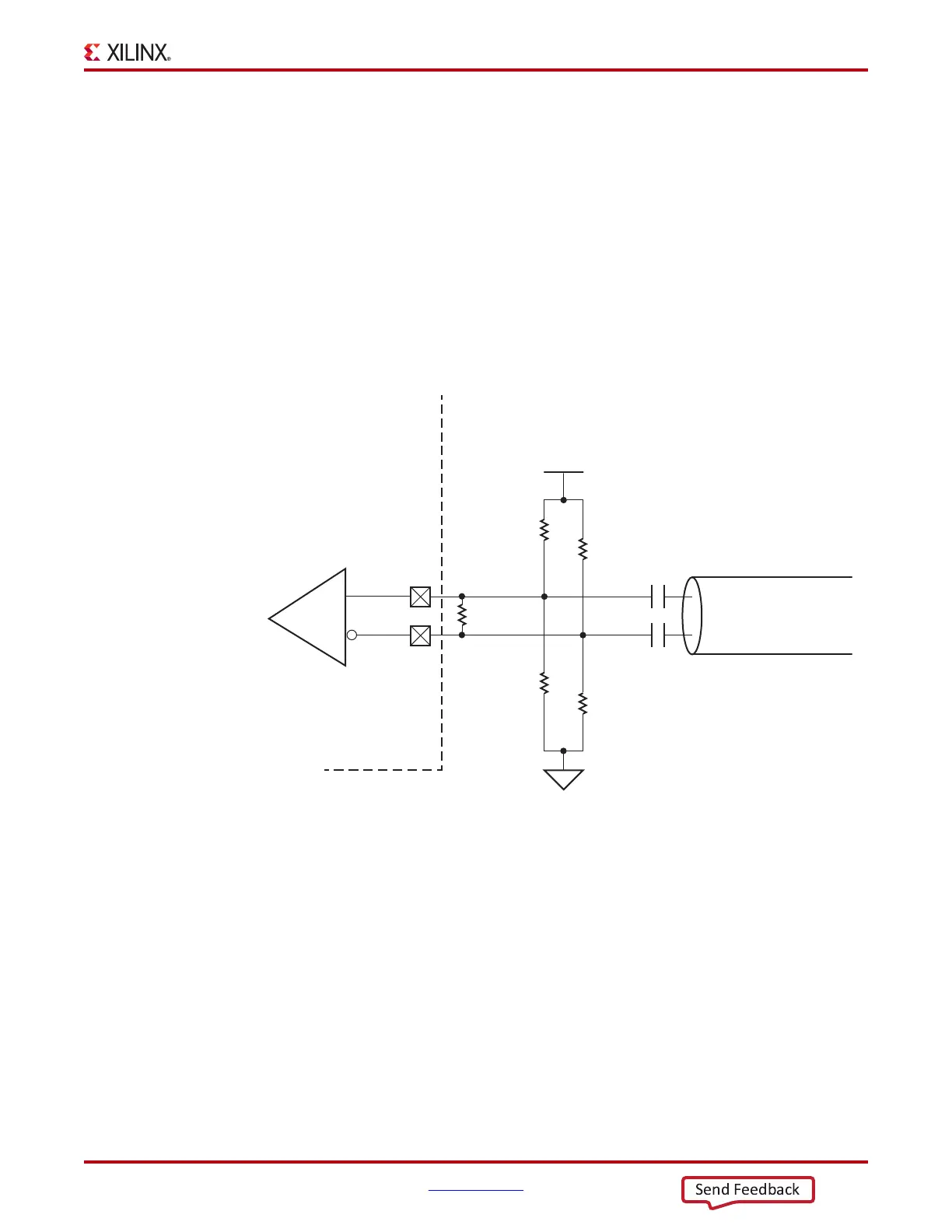
One way to accomplish the above criteria is to use an external circuit that both AC-couples
and DC-biases the input signals. Figure 1-72 shows an example circuit for providing an
AC-coupled and DC-biased circuit for a differential clock input. R
DIFF
provides the 100Ω
differential receiver termination because the internal DIFF_TERM is set to FALSE. To
maximize the input noise margin, all R
BIAS
resistors should be the same value, essentially
creating a V
ICM
level of V
CCO
/2. Resistors in the 10k–100KΩ range are recommended. The
typical values for the AC coupling capacitors C
AC
are in the range of 100 nF. All
components should be placed physically close to the FPGA inputs.
X-Ref Target - Figure 1-7 2
Figure 1-72: Example Circuit for AC-Coupled and DC-Biased Differential
Clock Input
V
CCO
FPGA
Differential
Transmission Line
C
AC
C
AC
R
BIAS
R
BIAS
R
BIAS
R
BIAS
R
DIFF
100Ω
N
P
LVDS or
LVDS_25
Input
Buffer
Differential Clock
Input to the FPGA
UG471_c1_72_050212