92 www.xilinx.com 7 Series FPGAs SelectIO Resources User Guide
UG471 (v1.10) May 8, 2018
Chapter 1: SelectIO Resources
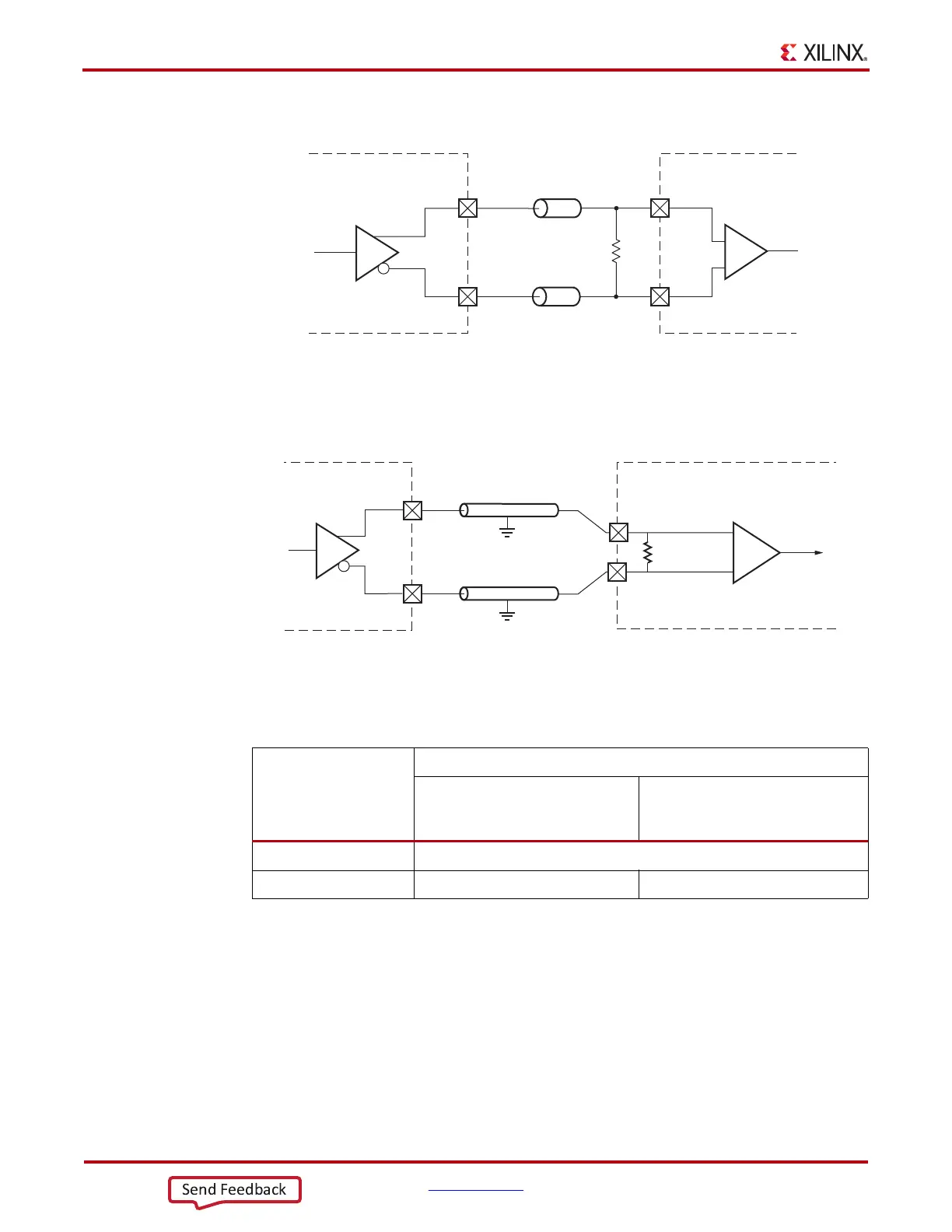
Figure 1-71 is an example of a differential termination for an LVDS or LVDS_25 receiver on
a board with 50Ω transmission lines.
Table 1-44 lists the available 7 series FPGA LVDS I/O standards and attributes supported.
It is acceptable to have differential inputs such as LVDS and LVDS_25 in I/O banks that are
powered at voltage levels other than the nominal voltages required for the outputs of those
standards (1.8V for LVDS outputs, and 2.5V for LVDS_25 outputs). However, these criteria
must be met:
• The optional internal differential termination is not used (DIFF_TERM = FALSE,
which is the default value).
• The differential signals at the input pins meet the V
IN
requirements in the
Recommended Operating Conditions table of the specific device family data sheet.
X-Ref Target - Figure 1-7 0
Figure 1-70: LVDS or LVDS_25 Receiver Termination
X-Ref Target - Figure 1-7 1
Figure 1-71: LVDS or LVDS_25 With DIFF_TERM Receiver Termination
Table 1-44: Allowed Attributes of the LVDS I/O Standards
Attributes
Primitives
IBUFDS, IBUFGDS,
IBUFDS_DIFF_OUT, or
IBUFGDS_DIFF_OUT
OBUFDS or OBUFTDS
IOSTANDARD LVDS (HP I/O Banks) or LVDS_25 (HR I/O Banks)
DIFF_TERM TRUE, FALSE N/A
ug471_c1_60_011811
+
–
External Termination
Z
0
IOB
IOB
LVD S
LVD S_25
LVD S
LVD S_25
Z
0
R
DIFF
= 2Z
0
= 100Ω
ug471_c1_61_011811
Data in
Z
0
= 50
Z
0
= 50
R
DIFF
= 100
LVDS
LVDS_25
LVDS
LVDS_25
+
–
0
0
IOB IOB