9.2 Port 1
9.2.1 Overview
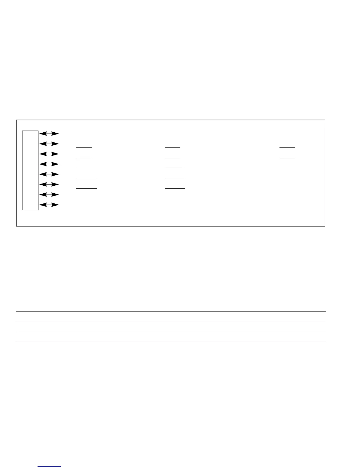
Port 1 is an 8-bit input/output port with the pin configuration shown in figure 9-1. All pins have
dual functions, except that in the single-chip mode pins 4, 3, and 2 do not have the WAIT, BREQ,
and BACK functions. (because the CPU does not access an external bus.)
Outputs from port 1 can drive one TTL load and a 90pF capacitive load. They can also drive a
Darlington transistor pair.
9.2.2 Port 1 Registers
Register Configuration: Table 9-2 lists the registers of port 1.
Table 9-2 Port 1 Registers
Name Abbreviation Read/Write Initial Value Address
Port 1 data direction register P1DDR W H'03 H'FF80
Port 1 data register P1DR R/W
*
1
Undetermined
*
2
H'FF82
Port 1 control register P1CR R/W H'87 H'FFFC
*1 Bits 1 and 0 are read-only.
*2 Bits 1 and 0 are undetermined. Other bits are initialized to “0.”
Pin Expanded Modes Single-Chip Mode
P1
7 / TMO P17 (input/output) / TMO (output) P17 (input/output) / TMO (output)
P1
6 / IRQ1 P16 (input/output) / IRQ1 (input) P16 (input/output) / IRQ1 (input)
P1
5 / IRQ0 P15 (input/output) / IRQ0 (input) P15 (input/output) / IRQ0 (input)
Port P1
4 / WAIT P14 (input/output) / WAIT (input) P14 (input/output)
1P1
3 / BREQ P13 (input/output) / BREQ (input) P13 (input/output)
P1
2 / BACK P12 (input/output) / BACK (output) P12 (input/output)
P1
1 / E P11 (input) / E (output) P11 (input) / E (output)
P1
0 / ø P10 (input) / ø (output) P10 (input) / ø (output)
Figure 9-1 Pin Functions of Port 1
142
Downloaded from Elcodis.com electronic components distributor

 Loading...
