Port 7 has Schmitt inputs. Outputs from port 7 can drive one TTL load and a 30pF capacitive
load. They can also drive a Darlington transistor pair.
9.8.2 Port 7 Registers
Register Configuration: Table 9-12 lists the registers of port 7.
Table 9-12 Port 7 Registers
Name Abbreviation Read/Write Initial Value Address
Port 7 data direction register P7DDR W H'00 H'FF8C
Port 7 data register P7DR R/W H'00 H'FF8E
1. Port 7 Data Direction Register (P7DDR)—H'FF8C
P7DDR is an 8-bit register that selects the direction of each pin in port 7. A pin functions as an
output pin if the corresponding bit in P7DDR is set to “1,” and as an input pin if the bit is cleared
to “0.”
P7DDR can be written but not read. An attempt to read this register does not cause an error, but
all bits are read as “1,” regardless of their true values.
At a reset and in the hardware standby mode, P7DDR is initialized to H'00, setting all pins for
input. P7DDR is not initialized in the software standby mode, so if a P7DDR bit is set to “1”
when the chip enters the software standby mode, the corresponding pin continues to output the
value in the port 7 data register.
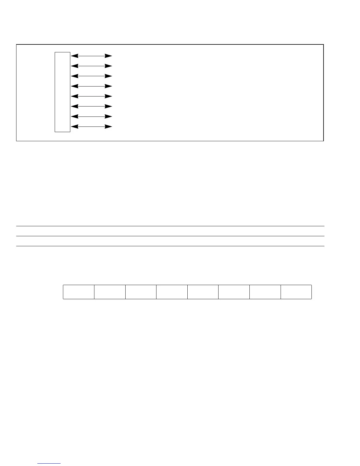
P77 (input/output) / FTOA1 (output)
P7
6 (input/output) / FTOB3 (output) / FTCI3 (input)
P7
5 (input/output) / FTOB2 (output) / FTCI2 (input)
Port P7
4 (input/output) / FTOB1 (output) / FTCI1 (input)
7P7
3 (input/output) / FTI3 (input) /TMRI (input)
P7
2 (input/output) / FTI2 (input)
P7
1 (input/output) / FTI1 (input)
P7
0 (input/output) / TMCI (input)
Bit 76543210
P7
7DDR P76DDR P75DDR P74DDR P73DDR P72DDR P71DDR P70DDR
Initial value 00000000
Read/Write WWWWWWWW
Figure 9-19 Pin Functions of Port 7
168
Downloaded from Elcodis.com electronic components distributor

 Loading...
