Table C-9 (e) Port 9 Port Read (Pin P97)
Setting Port Read Data
Clock input enable Input clock value
Clock output enable Output clock value
Clock input/output DDR = 0 Pin value
enable DDR = 1 DR value
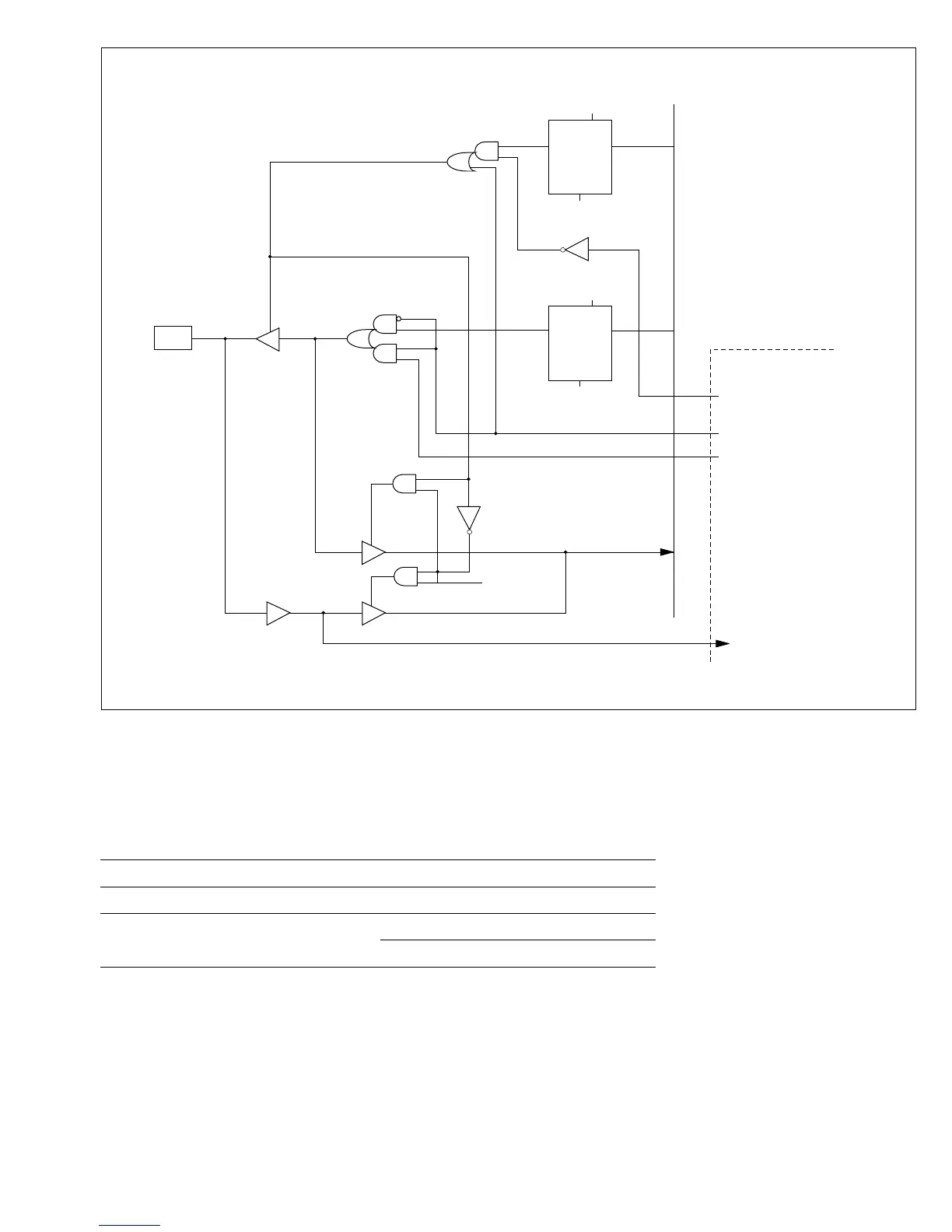
RP9
P9
7
WP9
SCI timer module
Clock input enable
WP9D:
WP9:
RP9:
Write to P9DDR
Write to Port 9
Read Port 9
Internal data bus (PDB15)
C
R
QD
P9 DR
7
C
R
QD
P9 DDR
7
Reset
Reset
WP9D
Clock output enable
Clock output
Clock input
Figure C-9 (e) Schematic Diagram of Port 9, Pin P97
428
Downloaded from Elcodis.com electronic components distributor

 Loading...
