1. Port 1 Data Direction Register (P1DDR)—H'FF80
P1DDR is an 8-bit register that selects the direction of each pin in port 1. A pin functions as an
output pin if the corresponding bit in P1DDR is set to “1,” and as an input pin if the bit is cleared
to “0.”
P1DDR can be written but not read. An attempt to read this register does not cause an error, but
all bits are read as “1,” regardless of their true values.
A reset initializes P1DDR to H'03, so that pins P11 and P10 carry clock outputs and the other pins
are set for input. In the hardware standby mode, P1DDR is cleared to H'00, stopping the clock
outputs. P1DDR is not initialized in the software standby mode, so if a P1DDR bit is set to “1”
when the chip enters the software standby mode, the corresponding pin continues to output the
value in the port 1 data register (or the ø or E clock).
2. Port 1 Data Register (P1DR)—H'FF82
P1DR is an 8-bit register containing the data for pins P17 to P10. When the CPU reads P1DR, for
output pins it reads the value in the P1DR latch, but for input pins, it obtains the pin status directly.
Note that when pins P11 and P10 are used for output, they output the clock signals (ø and E), not
the contents of P1DR. If the CPU reads Pl1 and Pl0 (when Pl1DDR = Pl0DDR = 1), it obtains the
clock values at the current instant.
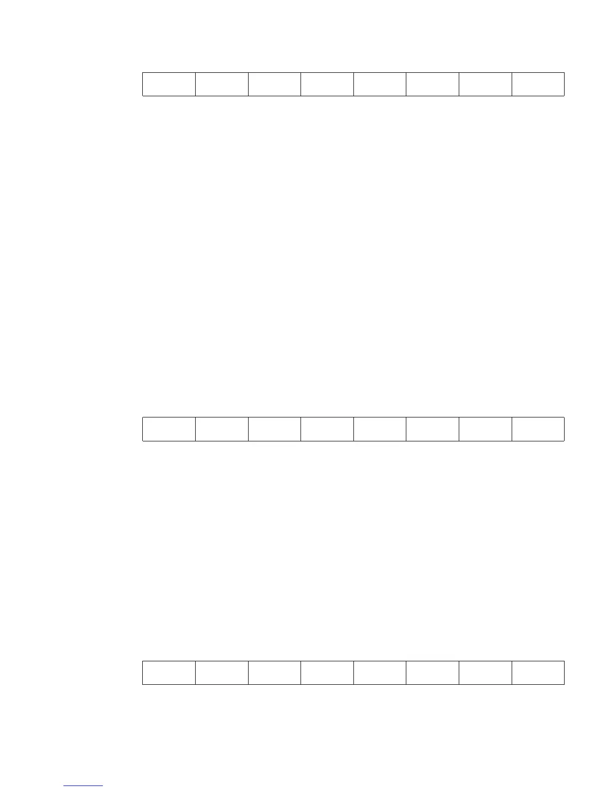
3. Port 1 Control Register (P1CR)—H'FFFC
Bit 76543210
P1
7DDR P16DDR P15DDR P14DDR P13DDR P12DDR P11DDR P10DDR
Initial value 00000011
Read/Write WWWWWWWW
Bit 76543210
P1
7 P16 P15 P14 P13 P12 P11 P10
Initial value 000000——
Read/Write R/W R/W R/W R/W R/W R/W R R
Bit 76543210
— IRQ
1E IRQ0E NMIEG BRLE — — —
Initial value 10000111
Read/Write — R/W R/W R/W R/W — — —
143
Downloaded from Elcodis.com electronic components distributor

 Loading...
