1.3 Pin Arrangements and Functions
1.3.1 Pin Arrangement
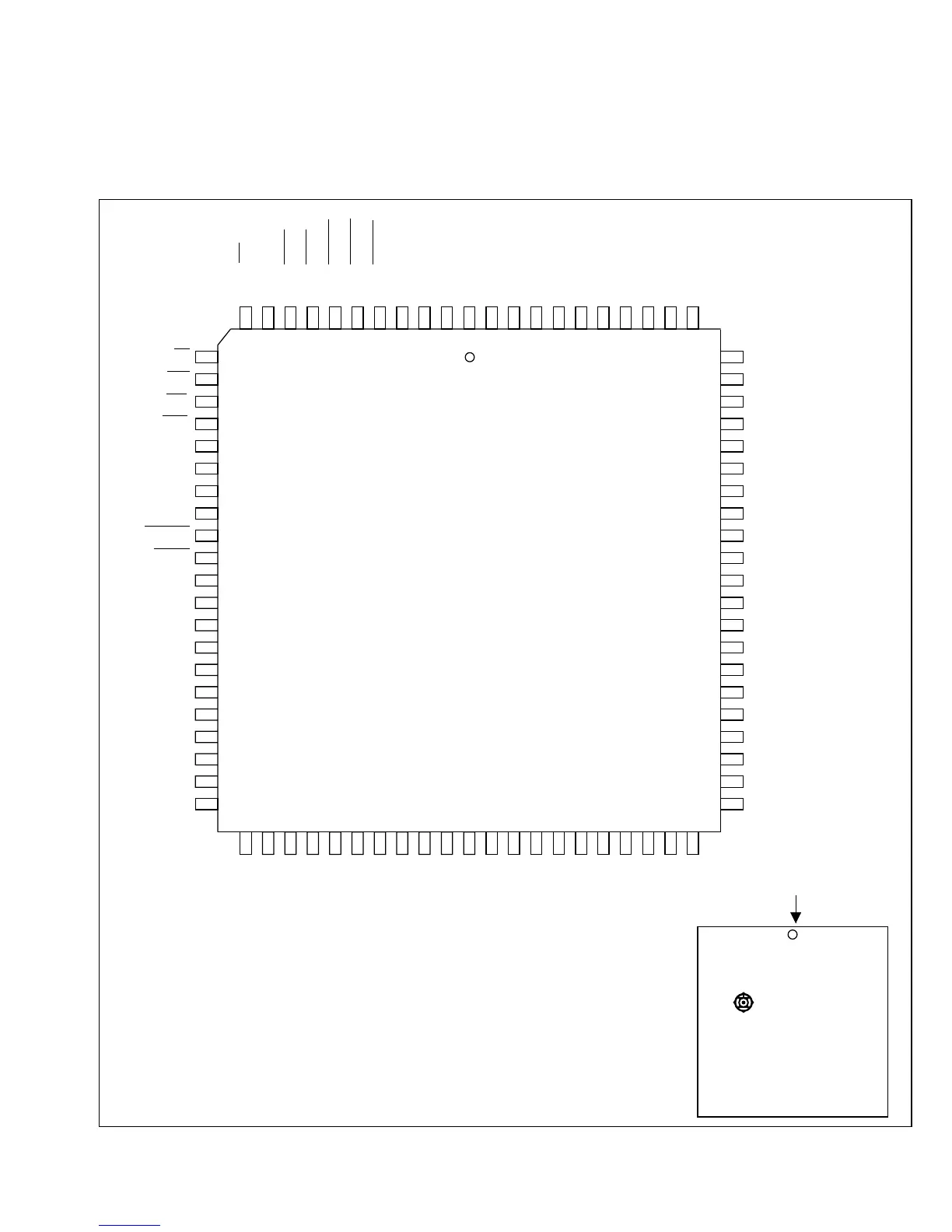
Figure 1-2 shows the pin arrangement of the CP-84 package. Figure 1-3 shows the pin
arrangement of the CG-84 package. Figure 1-4 shows the pin arrangement of the FP-80A package.
1 pin
P2 /R/W
P2 /DS
P2 /RD
P2 /WR
V
MD
MD
MD
STBY
RES
NMI
NC
V
P3 /D
P3 /D
P3 /D
P3 /D
P3 /D
P3 /D
P3 /D
P3 /D
1
2
3
4
cc
0
1
2
ss
0
1
2
3
4
5
6
7
0
1
2
3
4
5
6
7
12
13
14
15
16
17
18
19
20
21
22
23
24
25
26
27
28
29
30
31
32
74
73
72
71
70
69
68
67
66
65
64
63
62
61
60
59
58
57
56
55
54
111098765432184838281807978777675
33 34 35 36 37 38 39 40 41 42 43 44 45 46 47 48 49 50 51 52 53
PLCC-84
H8/532
HD6475328CP
JAPAN
AV
P8 /AN
P8 /AN
P8 /AN
P8 /AN
P8 /AN
P8 /AN
P8 /AN
P8 /AN
AV
V
P7 /FTOA
P7 /FTOB /FTCI
P7 /FTOB /FTCI
P7 /FTOB /FTCI
P7 /FTI /TMRI
P7 /FTI
P7 /FTI
P7 /TMCI
V
P6 /A
cc
77
66
55
44
33
22
11
00
ss
ss
7
6
5
4
3
2
1
0
cc
3
1
3
2
1
3
2
1
3
2
1
19
P2 /AS
P1 /TMO
P1 /IRQ
P1 /IRQ
P1 /WAIT
P1 /BREQ
P1 /BACK
P1 /E
P1 /ø
V
XTAL
EXTAL
V
P9 /SCK
P9 /RXD
P9 /TXD
P9 /PW
P9 /PW
P9 /PW
P9 /FTOA
P9 /FTOA
0
7
6
5
4
3
2
1
0
ss
ss
7
6
5
4
3
2
1
0
3
2
1
3
2
1
0
P4 /A
P4 /A
P4 /A
P4 /A
P4 /A
P4 /A
P4 /A
P4 /A
V
V
P5 /A
P5 /A
P5 /A
P5 /A
P5 /A
P5 /A
P5 /A
P5 /A
P6 /A
P6 /A
P6 /A
0
1
2
3
4
5
6
7
ss
ss
08
19
210
311
412
513
614
715
013
114
215
0
1
2
3
4
5
6
7
5
Figure 1-2 Pin Arrangement (CP-84, Top View)
Downloaded from Elcodis.com electronic components distributor

 Loading...
