Access to External Devices: The access cycle consists of three states. The data bus is 8 bits
wide. Figure 3-10 (a) and (b) shows the external access cycle. Additional wait states (Tw) can be
inserted by the wait-state controller (WSC).
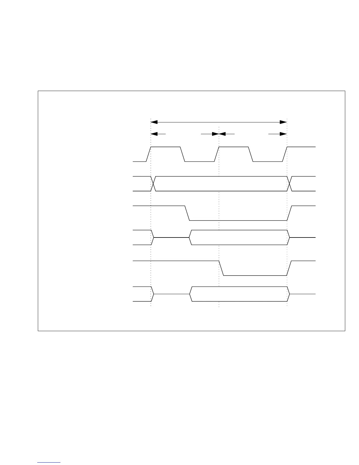
3.7.2 On-Chip Memory Access Cycle
T state
Memory cycle
1 T state2
ø
Internal address bus
Internal Read signal
Internal data bus
(Read access)
Internal Write signal
Read data
Address
Write data
Internal data bus
(Write access)
Figure 3-6 On-Chip Memory Access Timing
64
Downloaded from Elcodis.com electronic components distributor

 Loading...
