Bit 2
OEA Description
0 Output compare A output is disabled. (Initial value)
1 Output compare A output is enabled.
Bits 1 and 0—Clock Select (CKS1 and CKS0): These bits select external clock input or one of
three internal clock sources for the FRC. External clock pulses are counted on the rising edge.
Bit 1 Bit 0
CKS1 CKS0 Description
0 0 Internal clock source (ø/4) (Initial value)
0 1 Internal clock source (ø/8)
1 0 Internal clock source (ø/32)
1 1 External clock source (counted on the rising edge)*
* Output enable bit (bit 3) must be cleared to “0.”
10.2.5 Timer Control/Status Register (TCSR)
The TCSR is an 8-bit readable and partially writable* register that selects the input capture edge
and output compare levels, and specifies whether to clear the counter on compare-match A. It also
contains four status flags.
The TCSR is initialized to H'00 at a reset and in the standby modes.
* Software can write a “0” in bits 7 to 4 to clear the flags, but cannot write a “1” in these bits.
Bit 7—Input Capture Flag (ICF): This status flag is set to “1” to indicate an input capture
event. It signifies that the FRC value has been copied to the ICR.
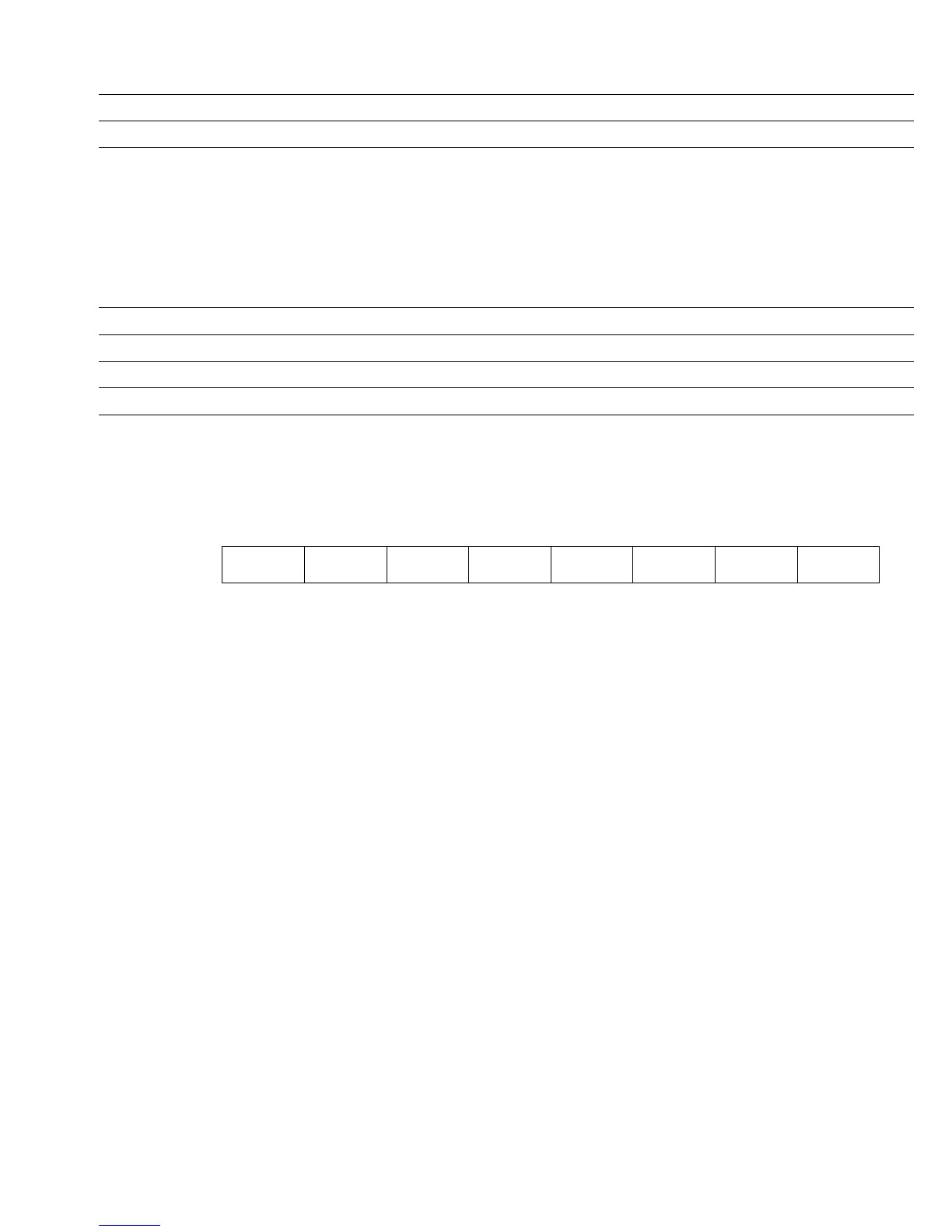
Bit 76543210
ICF OCFB OCFA OVF OLVLB OLVLA IEDG CCLRA
Initial value 00000000
Read/Write R/(W)* R/(W)* R/(W)* R/(W)* R/W R/W R/W R/W
185
Downloaded from Elcodis.com electronic components distributor

 Loading...
