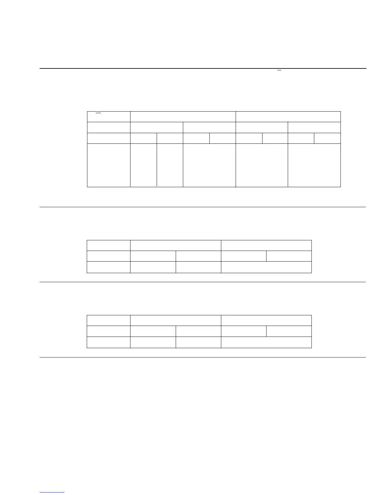
Table 9-16 shows how the functions of the pins of port 9 are selected.
Table 9-16 Port 9 Pin Functions
Pin Selection of Pin Functions
P9
7 / The function depends on the communication mode bit (C/A) and the clock enable 1
SCK and 2 bits (CKE1 and CKE0) of the serial control register (SCR) of the serial
communication interface as follows:
C/A 0 1
CKE1 0 1 0 1
CKE0 01010101
Pin function P9
7 SCI SCI external SCI internal SCI external
input internal clock input clock output clock input
or clock
output* output
* Input or output is selected by the P9
7DDR bit.
P9
6 / RXD The function depends on the receive enable bit (RE) of the serial control register
(SCR) and on the P9
6DDR bit as follows:
RE 0 1
P9
6DDR0101
Pin function P9
6 input P96 output RXD input
P9
5 / TXD The function depends on the transmit enable bit (TE) of the serial control register
(SCR) and on the P9
5DDR bit as follows:
TE 0 1
P9
5DDR0101
Pin function P9
5 input P95 output TXD output
175
Downloaded from Elcodis.com electronic components distributor

 Loading...
