intdo
87C51GBHARDWARE DESCRIPTION
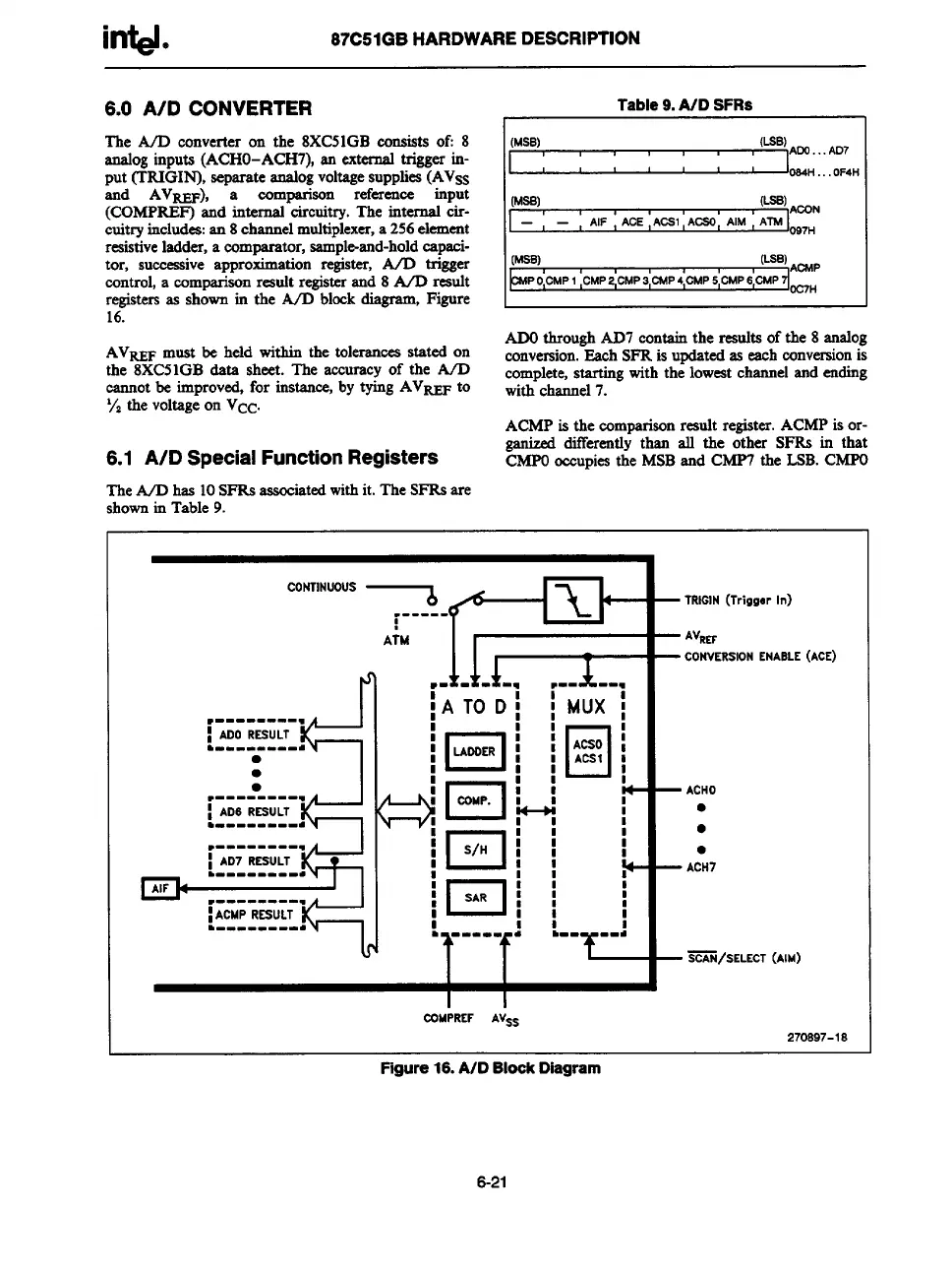
6.0 A/D CONVERTER
TheA/D converter on the 8XC51GBconsists of: 8
analoginputs (ACHO-ACH7),an external trigger in-
put (TRIGIN), separate analogvoltagesupplies(AV~
and AV~), a comparison reference input
(COMPREF)and internal circuitry. The internal cir-
cuitryincludea:an 8channelmultiplexer,a 256element
reaiativeladder,a comparator, sample-and-holdcapaci-
tor, successiveapproximation register, A/D trigger
control,a comparisonresult registerand 8 MD result
registersas shownin the A/D blcck diagram, Figure
16.
AV~F must be held within the tolerancesstated on
the 8XC51GBdata sheet. The accuracyof the A/D
cannot be improved,for instance,by tying AVREFto
y, the voltageon VCC.
6.1 A/D Special Function Registers
TheA/D has 10SFRS
associatedwithit. The SFR6are
shownin Table 9.
Table9.AID SFRa
(MSB)
(LBB)
~~;::z’”
(MSB)
(LsB)
ACQN
——
AIF , ACE ACS1 ACSO AIM , ATM
OS7H
(MSB)
(LSB)
ACMP
CC7H
ADOthroughAD7 contain the results of the 8 analog
conversion.Each SFR is updatedas eachcmversionis
complete,starting with the lowestchannel and ending
with channel7.
ACMPis the comparisonresult register.ACMPis or-
- differently than all the other SFRSin that
CMPOoccupiesthe MSBand CMP7 the LSB.CMPO
‘O”’’””O”sT ~
It
TRIGIN(Trigger In)
------
8
+
*---------
I
!...- – ,
: ADORESULT
b--------a
I I i I
AfUWRi I I IA’=~’JI I
●
●
●✍✍✍✍✍✍✍✍✍
; AD6RESULT
Ak
b--------a
4
‘1 — I
I
!I-71!
I I
b ----- ●
If
AVm
CONVERSIONENABLE
, ACHO
●
.
●
ACH7
?i’EZi4\SELECT(AIM)
(ACE)
COh4PREFAVs5
270897-1S
Figure16.A/D BlockDiagram
6-21