Because RFL™ and Hubbell® have a policy of continuous product improvement, we reserve the right to change designs and specifications without notice.
M-DACS-T1 RFL Electronics Inc.
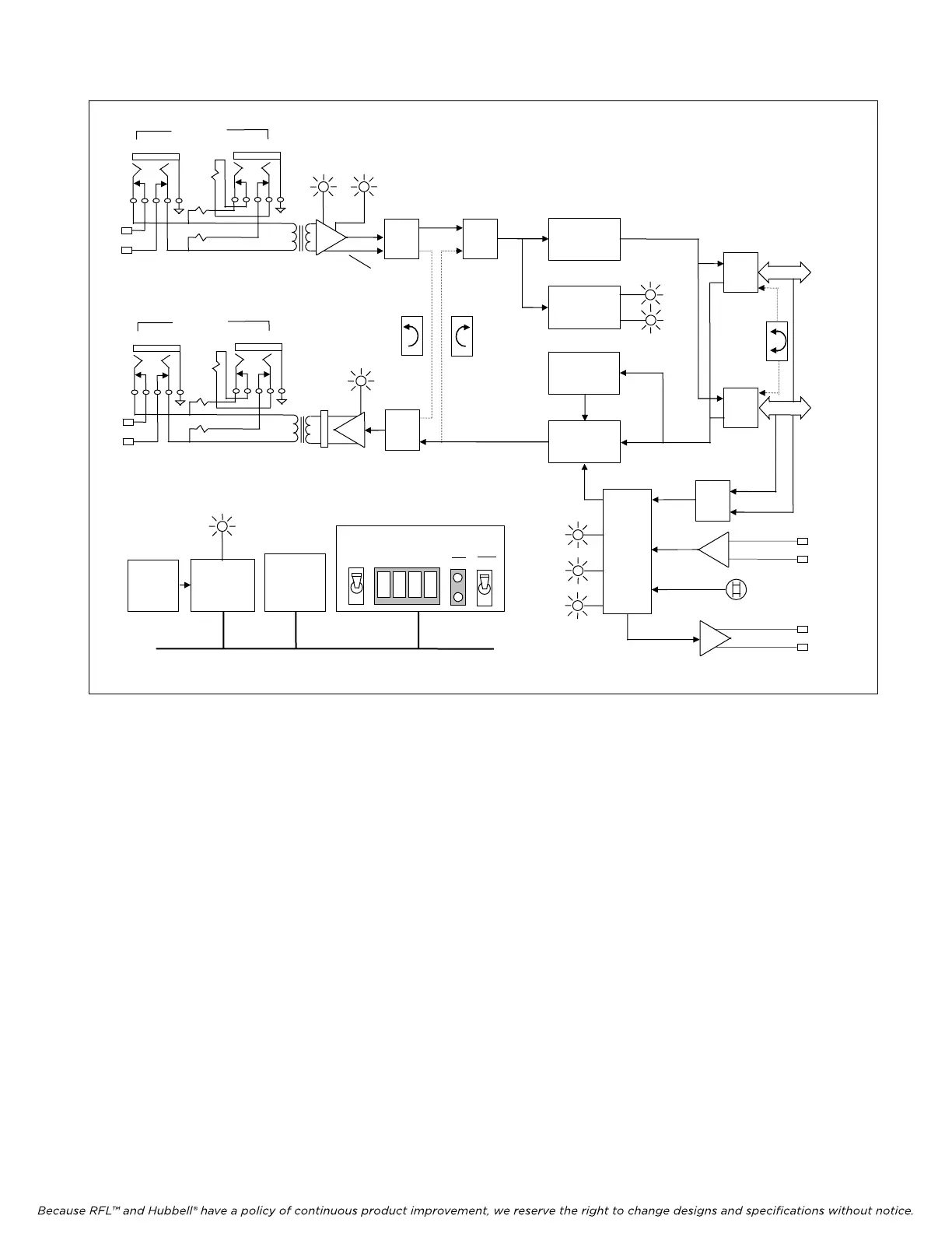
Jitter
Buffer
Select
Multiplexer
Demultiplexer
Frame
Synchronization
Timing
Select
Micro-
processor
Non-
volatile
memory
Front Panel User Interface
Figure 2-15. Functional diagram, CM4 Common Module, Communications Control
CM4 Status and Control Bus
Select
LOOP
EXT
INT
Loop or
Through
External
Internal
oscillator
Bus
Switch
A
Bus
Switch
B
Bus B
Bus A
FRM
ERR
Frame
Overhead
To/From
Channel
Modules
External
Timing
Input
Timing
Output
(RS-422)
RX IN BPV
Line Recovered
Receiver Timing
Data
Select
“DeMUX”
Bus
Equipment
Loopback
Line
Loopback
LBO
TX OUT
Line
Driver
LPBK
GROUP FUNCTION
ON
OFF
SET
NEXT
RS-232
Serial
Port
Payload
Loopback
110
430
430
EQUIP
MON
T1 IN
T1 Input
110
430
430
EQUIP
MON
T1 IN
1 Output T
October 16, 2012 2-28 (973) 334-3100