Because RFL™ and Hubbell® have a policy of continuous product improvement, we reserve the right to change designs and specifications without notice.
“B” BUS
“A” BUS
DI-A
CM4
DI-B
CM4
DACS MODULE
5
6
7
1
2 4
CHANNEL
MODULE
Module
Adapter
CHANNEL
MODULE
Module
Adapter
CHANNEL
MODULE
Module
Adapter
Line
I/O
or
OIA
Line
I/O
or
OIA
Line
I/O
or
OIA
Line
I/O
or
OIA
MA-235
Comms. I/O
“SCB” BUS
External
Timing:
IN/OUT
RS-485
RS-232
Remote Port
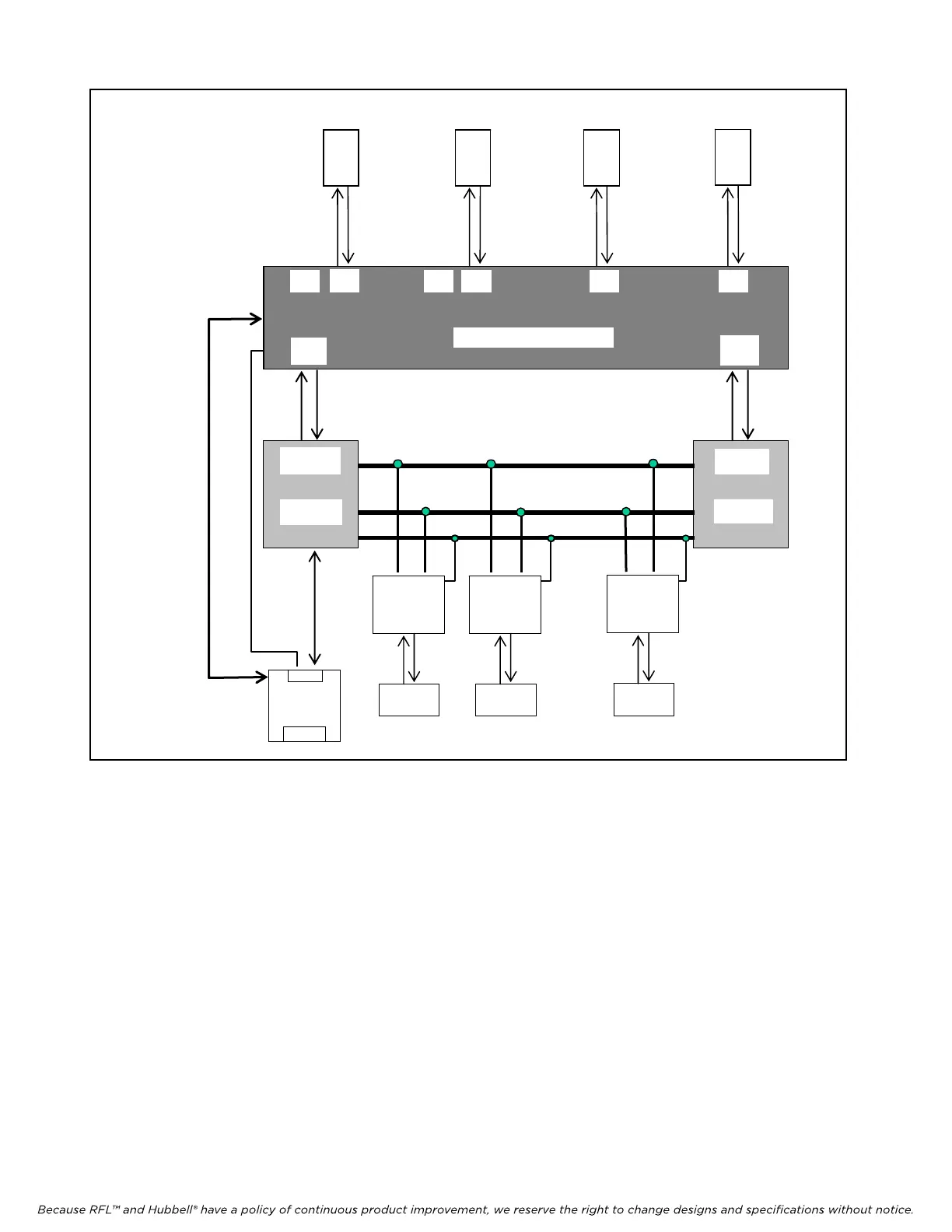
Figure
3-2. M-DACS System Block Diagram
Each DACS module is composed of two boards, a processor board and a framer board. The Processor
board controls the entire DACS module and is required to initialize and monitor the Framer board. The
Framer board performs all of the real-time T1 processing.
M-DACS-T1 RFL Electronics Inc.
October 25, 2004 3-3 (973) 334-3100