Because RFL™ and Hubbell® have a policy of continuous product improvement, we reserve the right to change designs and specifications without notice.
RFL NCM RFL Electronics Inc.
Novem
b
er 1, 2012 6 (973) 334-3100
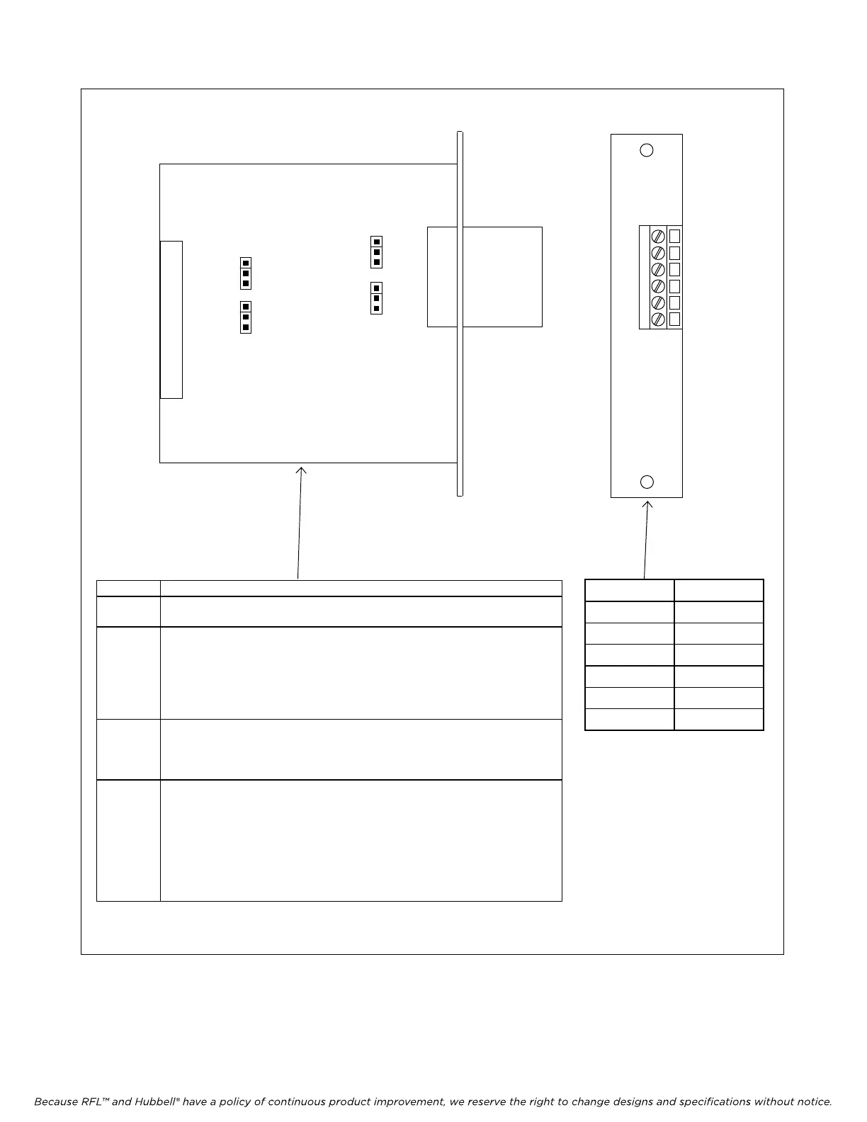
TB1 Pin No. Function
1 TDB (+)
2 TDA (-)
3 GND
4 RDB (+)
5 RDA (-)
6 GND
Figure 2. MA-485 Module adapter, jumper functions and TB1 pinouts
MA485
TB1
1
2
3
4
5
6
Jumper Function
J1 Selects 2W or 4W operation
J2 In 4W operation, selects MARK or HI-Z as follows:
In “MARK” position, forces the transmission of “All Marks”
when data is not being transmitted.
In “HI-Z” position, forces the output to a “high impedance” when data
is not being transmitted.
J3 In 4W operation, selects Rx path termination as follows:
In “IN” position, a 120Ω termination is inserted in the Rx path.
In “OUT” position, the Rx path remains unterminated.
J4 In 4W operation, selects Tx path termination as follows:
In “IN” position, a 120Ω termination is inserted in the Tx path.
In “OUT” position , the Tx path remains unterminated
In 2W operation, selects Tx & Rx path termination as follows:
In “IN” position, a 120Ω termination is inserted in the Tx & Rx paths.
In “OUT” position, the Tx & Rx paths remain unterminated.
4W IDLE OUT
MARK
HI-Z
4W
2W
TERMINATION
OUT
IN
OUT
IN
J2
J1
J4
J3
Note: For 2W use pins 1, 2, 3
For 4W use pins
1, 2, 4, 5, 6