Date Code 20090715 SEL-421 Relay
List of Figures
User’s Guide
Figure 1.1 SEL-421 Functional Overview........................................................................................... U.1.2
Figure 1.2 Protecting a Line Segment With M
IRRORED BITS Communications on a Fiber Channel.. U.1.8
Figure 1.3 Single Circuit Breaker Configuration (ESS := 1)............................................................... U.1.9
Figure 1.4 Single Circuit Breaker Configuration With Line Breaker CTs (ESS := 2) ........................ U.1.9
Figure 1.5 Double Circuit Breaker Configuration (ESS := 3) ............................................................. U.1.9
Figure 1.6 Double Circuit Breaker Configuration With Bus Protection (ESS := 4).......................... U.1.10
Figure 1.7 Tapped Line (ESS := Y) ................................................................................................... U.1.10
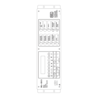
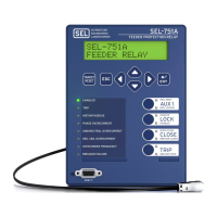
Figure 2.1 Horizontal Front-Panel Template (a); Vertical Front-Panel Template (b).......................... U.2.3
Figure 2.2 Rear 3U Template, Fixed Terminal Block Analog Inputs.................................................. U.2.4
Figure 2.3 Rear 3U Template, Connectorized Analog Inputs ............................................................. U.2.4
Figure 2.4 Standard Control Output Connection................................................................................. U.2.8
Figure 2.5 Hybrid Control Output Connection.................................................................................... U.2.8
Figure 2.6 Fast Hybrid Control Output Connection, INT5 (INT8) ..................................................... U.2.9
Figure 2.7 Fast Hybrid Control Output Connection, INT4 ................................................................. U.2.9
Figure 2.8 Fast Hybrid Control Output Typical Terminals, INT5 (INT8)......................................... U.2.10
Figure 2.9 Precharging Internal Capacitance of Fast Hybrid Output Contacts, INT5 (INT8) .......... U.2.10
Figure 2.10 INT1 I/O Interface Board................................................................................................. U.2.12
Figure 2.11 INT2 I/O Interface Board................................................................................................. U.2.13
Figure 2.12 INT3 I/O Interface Board................................................................................................. U.2.13
Figure 2.13 INT4 I/O Interface Board................................................................................................. U.2.13
Figure 2.14 INT5 I/O Interface Board................................................................................................. U.2.13
Figure 2.15 INT6 I/O Interface Board................................................................................................. U.2.13
Figure 2.16 INT7 I/O Interface Board................................................................................................. U.2.13
Figure 2.17 INT8 I/O Interface Board................................................................................................. U.2.13
Figure 2.18 Chassis Key Positions for I/O Interface Boards............................................................... U.2.16
Figure 2.19 Major Component Locations on the SEL-421 Main Board A (or B)............................... U.2.19
Figure 2.20 J18 Header—Password and Breaker Jumpers.................................................................. U.2.20
Figure 2.21 Major Component Locations on the SEL-421 INT1 (or INT2) I/O Board...................... U.2.23
Figure 2.22 Major Component Locations on the SEL-421 INT3 I/O Board....................................... U.2.24
Figure 2.23 Major Component Locations on the SEL-421 INT4 I/O Board....................................... U.2.25
Figure 2.24 Major Component Locations on the SEL-421 INT5 (or INT8) I/O Board...................... U.2.26
Figure 2.25 Major Component Locations on the SEL-421 INT6 (or INT7) I/O Board...................... U.2.27
Figure 2.26 SEL-421 Chassis Dimensions .......................................................................................... U.2.31
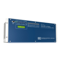
Figure 2.27 3U Rear Panel, Main Board A ......................................................................................... U.2.32
Figure 2.28 3U Rear Panel, Main Board A, Connectorized ................................................................ U.2.32
Figure 2.29 4U Rear Panel, Main Board A, Without Optional I/O ..................................................... U.2.33
Figure 2.30 4U Rear Panel, Main Board A, INT5 I/O Interface Board............................................... U.2.33
Figure 2.31 4U Rear Panel, Main Board B, INT8 I/O Interface Board............................................... U.2.33
Figure 2.32 5U Rear Panel, Main Board B, INT3 and INT1 I/O Interface Board .............................. U.2.34
Figure 2.33 5U Rear Panel, Main Board A, INT4 and INT1 I/O Interface Board .............................. U.2.34
Figure 2.34 5U Rear Panel, Main Board A, INT6 and INT4 I/O Interface Board .............................. U.2.35
Figure 2.35 5U Rear Panel, Main Board B, INT2 and INT7 I/O Interface Board .............................. U.2.35
Figure 2.36 Rear-Panel Symbols ......................................................................................................... U.2.36
Figure 2.37 Screw Terminal Connector Keying .................................................................................. U.2.37
Figure 2.38 Rear-Panel Receptacle Keying, SEL-421......................................................................... U.2.38
Figure 2.39 PS30 Power Supply Fuse Location .................................................................................. U.2.41
Figure 2.40 Control Output OUT108 .................................................................................................. U.2.44
Figure 2.41 SEL-421 to Computer—D-Subminiature 9-Pin Connector ............................................. U.2.47
Figure 2.42 Example Ethernet Panel With Fiber-Optic Ports.............................................................. U.2.48
Figure 2.43 Two 10/100BASE-T Port Configuration.......................................................................... U.2.49
Figure 2.44 100BASE-FX and 10/100BASE-T Port Configuration.................................................... U.2.49
Courtesy of NationalSwitchgear.com