Comparator (COMP) RM0453
632/1454 RM0453 Rev 2
21.6.3 COMP register map
The following table summarizes the comparator register map en reset values.
Refer to Section 2.6 for the register boundary addresses.
Bits 3:2 PWRMODE[1:0]: COMP2 power mode
These bits are set and cleared by software. They control the power and speed of COMP2.
00: High speed
01: Medium speed
10: Medium speed
11: Ultra low-power
Bit 1 Reserved, must be kept at reset value.
Bit 0 EN: COMP2 enable
This bit is set and cleared by software. It switches COMP2 on.
0: COMP2 switched off
1: COMP2 switched on
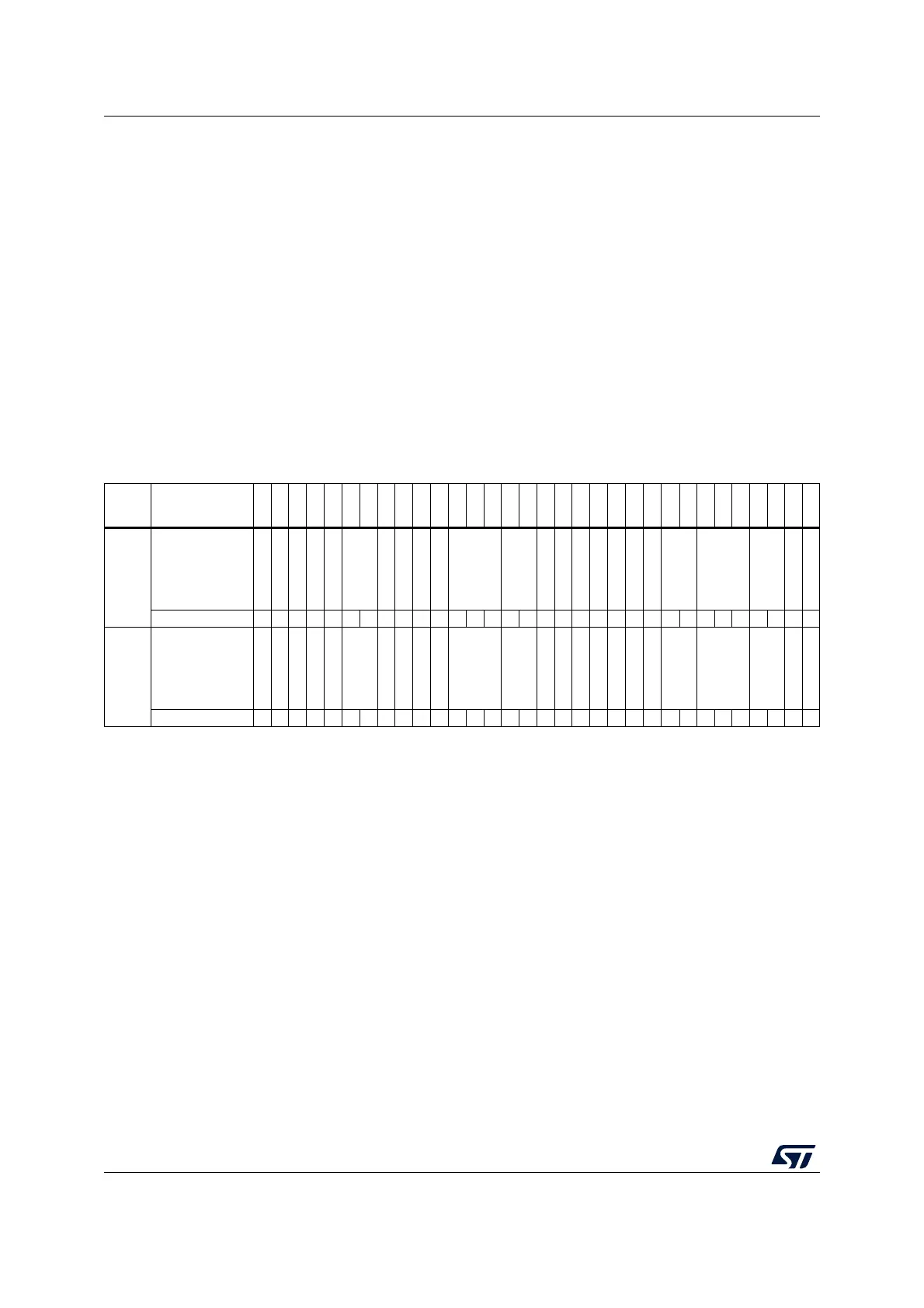
Table 128. COMP register map and reset values
Offset Register name
31
30
29
28
27
26
25
24
23
22
21
20
19
18
17
16
15
14
13
12
11
10
9
8
7
6
5
4
3
2
1
0
0x00
COMP1_CSR
LOCK
VALUE
Res.
Res.
Res.
INMESEL[1:0]
Res.
SCALEN
BRGEN
Res.
BLANKING[2:0]
HYST[1:0]
POLARITY
Res.
Res.
Res.
Res.
Res.
Res.
INPSEL[1:0]
INMSEL[2:0]
PWRMODE[1:0]
Res.
EN
Reset value 00 00 00 000000 0000000 0
0x04
COMP2_CSR
LOCK
VALUE
Res.
Res.
Res.
INMESEL[1:0]
Res.
SCALEN
BRGEN
Res.
BLANKING[2:0]
HYST[1:0]
POLARITY
Res.
Res.
Res.
Res.
Res.
WINMODE
INPSEL[1:0]
INMSEL[2:0]
PWRMODE[1:0]
Res.
EN
Reset value 00 00 00 000000 00000000 0

 Loading...


