True random number generator (RNG) RM0453
634/1454 RM0453 Rev 2
22.3 RNG functional description
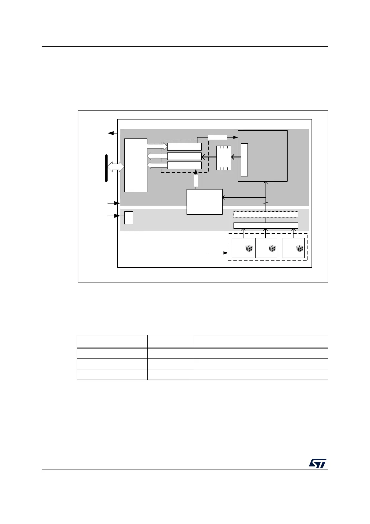
22.3.1 RNG block diagram
Figure 98 shows the RNG block diagram.
Figure 98. RNG block diagram
22.3.2 RNG internal signals
Table 129 describes a list of useful-to-know internal signals available at the RNG level, not
at the STM32 product level (on pads).
MSv42098V2
True RNG
RNG_CR
RNG_SR
AHB
interface
control
status
RNG_DR
data
Analog
noise
source 1
Banked Registers
Sampling (x N) + XOR
DIV
Analog noise source
Fault detection
Clock checker
Health tests
1-bit
CONDRST
Alarms
...
Analog
noise
source 2
Analog
noise
source N
4x32-bit
FIFO
Conditioning logic
128-bit data output
en_osc
rng_it
rng_hclk
rng_clk
AHB clock domain
RNG clock domain
Post-processing (optional)
32-bit AHB bus
Table 129. RNG internal input/output signals
Signal name Signal type Description
rng_it Digital output RNG global interrupt request
rng_hclk Digital input AHB clock
rng_clk Digital input RNG dedicated clock, asynchronous to rng_hclk

 Loading...


