Description Of Specific Functions 99
V560 Series High Performance Closed-Loop Vector Inverter User Manual
4: 2 wire Control 2/AI1 setting
Refer to Figure 7-2-B for the application wiring diagram, and refer to Table 7-1 for macro- related parameters.
5: 3 wire control 1/AI1 setting
Refer to Figure 7-3 for the application wiring diagram, and refer to Table 7-1 for macro- related parameters.
Table 7-1: Table Application Macro Association Self-Setting Parameters
Parameters
Application
Macro 1
Application
Macro 2
Application
Macro 3
Application
Macro 4
Application
Macro 5
Remarks
F0.1.15 0 0 0 0 0 Locked
F0.1.16 0 0 0 0 0 Locked
F0.1.18 1.00 1.00 1.00 1.00 1.00 Locked
F0.2.25 2 (0~2) 3 9 9 9 Locked
F0.3.33 0 0 1 1 1 Locked
F0.3.35 — — 0 1 2 Locked
F0.4.37 0 0 0 0 0 Locked
F0.4.38 0 0 0 0 0 Locked
F3.0.01 — — — — 19 Locked
F3.0.02 — — 7 7 7 Locked
F3.0.03 — — 8 8 8 Locked
F3.0.04 13 13 13 13 13 Locked
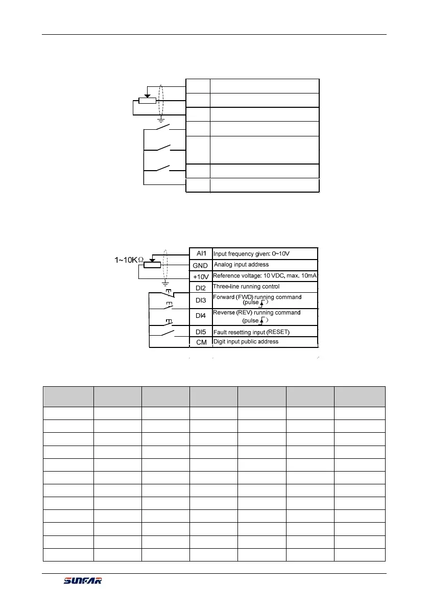
Figure 7-3 3 wire control 1/AI1 setting wiring diagram
AI1
Input frequency given: 0~10V
GND
Analog input address
+10V
Reference voltage:10 VDC, max. 10mA
DI3
Switch disengaged: FWDcommand
Switch engaged: REV command
DI4
Running command
DI5
Fault resetting input (RESET)
1~10KO
CM
Digit input public address
Figure 7-2-B 2 wire control 2/AI1 setting wiring diagram
 Loading...