Description Of Specific Functions 181
V560 Series High Performance Closed-Loop Vector Inverter User Manual
7.36 COMPENSATION PID (1MS CONTROL CYCLE) (GROUP F9.0)
F9.0.09 Analog input minimum
value is 0%
Setting range: 0.0V~[F9.0.10]/
AI2:0.0mA~[F9.0.10]
Factory default: 0.0
F9.0.10 Analog input maximum
value is 100%
Setting range: [F9.0.09]~10.00V/
AI2:[F9.0.09] ~20.00mA
Factory default: 10.00
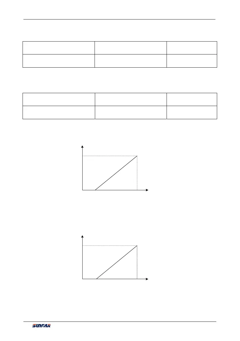
When the compensation PID setting source channel selects the analog channel input, this group of
parameters can be used to modify the correspondence relationship between the compensation PID set value
and the analog pot. The correspondence relationship is shown in Figure 7-65.
F9.0.13 Feedback input actual
value is 0%
Setting range: 0.0V~[F9.0.14]/
AI2:0.0mA~[F9.0.14]
Factory default: 0.0
F9.0.14 Feedback input actual
value is 100%
Setting range: [F9.0.13]~10.00V/
AI2:[F9.0.13] ~20.00mA
Factory default: 10.00
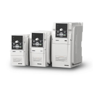
This group of parameters can be used to modify the correspondence relationship between the compensation
PID feedback value and the analogy port.The correspondence relationship is shown in Figure 7-66.
Analog Input
quantity
[F9.0.10]
0%
100%
Compensation PID set value
[F9.0.09]
Analog feedback
quantity
[F9.0.14]
0%
100%
Compensation PID feedback value
[F9.0.13]
Figure 7-65 Sketch of compensation
PID set value definition
Figure 7-66 Sketch of compensation
PID feedback value definition