Functional Parameter Table
V560 Series High Performance Closed-Loop Vector Inverter User Manual
92
6.2.56 TERMINAL STATUS AND VARIABLE
Function
Code
Name
Setting Range and
Description
Minimu
m Unit
Factory
Default
Change
Limit
d1.0.00 Terminal input (DI1~DI10) Segment marker - - R
d1.0.01 Terminal input (EDI1~EDI10) Segment marker - - R
d1.0.02 Pulse input (Fin) 0.0~100.00KHz 0.01 R
d1.0.03 Analog input AI1 0.00~10.00V 0.01 R
d1.0.04 Analog input AI2 0.00~20.00mA 0.01 R
d1.0.05 Analog input AI3 -10.00~10.00V 0.01 R
d1.0.06
Digital signal output (DO1~DO4,
EDO1~ EDO6)
Segment marker - - R
d1.0.07
Relay contact output (RO1~RO4,
ERO1~ERO6)
Segment marker - - R
d1.0.08
Frequency output Fout (indicating
the duty ratio in the case of PWM
signal output)
0.0~100.0KHz 0.01 R
d1.0.09 Analog output AO1 0.00~10.00V 0.01 R
d1.0.10 Analog output AO2 0.00~10.00V 0.01 R
6.2.57 COUNTER TIMER VALUE
Function
Code
Name Setting Range and Description
Minimu
m Unit
Factory
Default
Change
Limit
d1.1.11 Counter 1 current value 0~65535 1 R
d1.1.12 Counter 2 current value 0~65535 1 R
d1.1.13 Timer 1 current value 0~65535 1 R
d1.1.14 Timer 2 current value 0~65535 1 R
d1.1.15 Timer 3 current value 0~65535 1 R
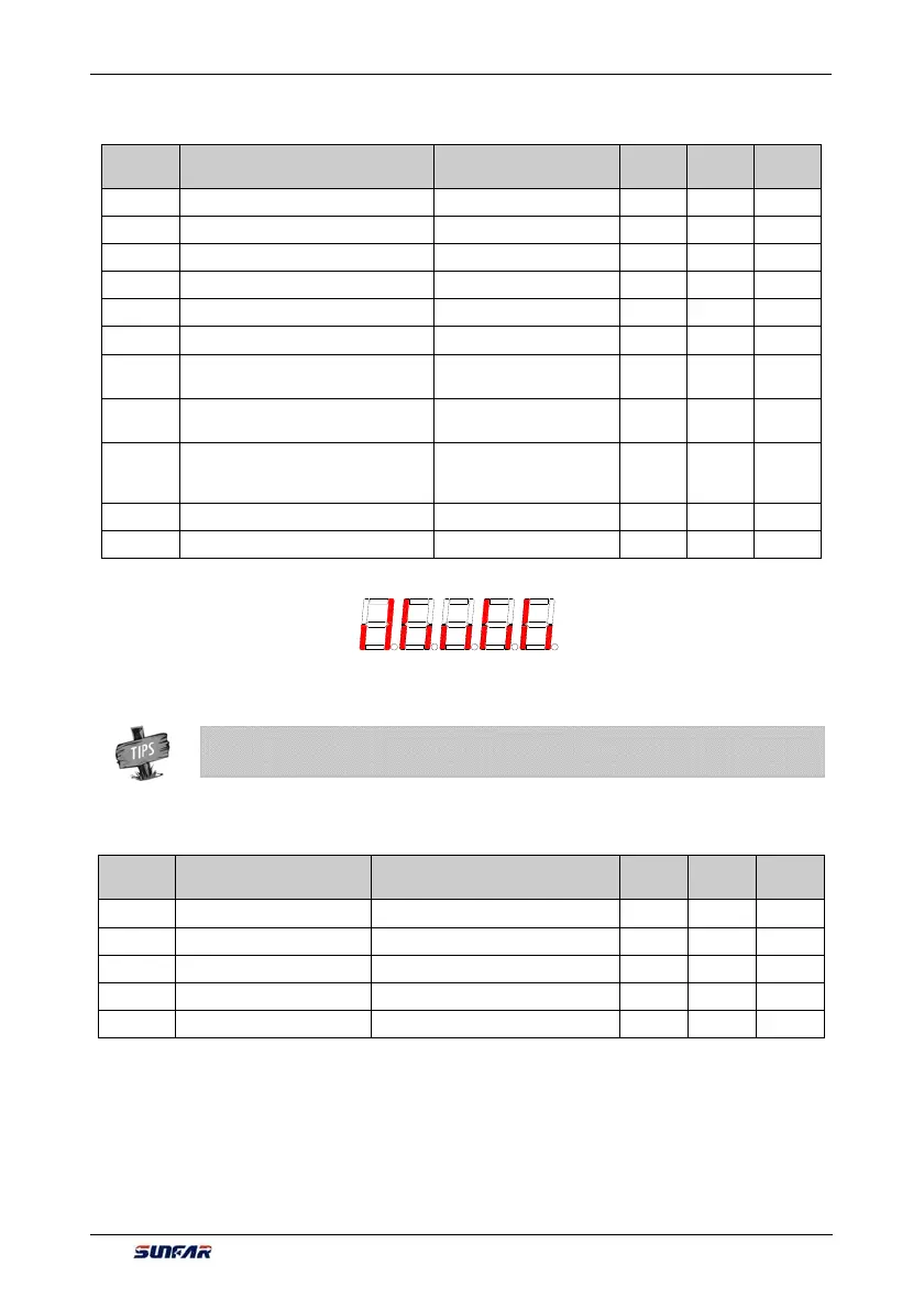
Figure 6-1 Terminal effective sketch
¾ As shown in Figure 6-1, DI2, DI3, DI7, DI9 terminal input is in effective status, and other
terminals are at void status.