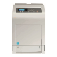
8-9
PWBs > Description for PWB
[CONFIDENTIAL]
9 BACNT O Analog DEV AC control signal
10 PAPERSEN2N I DC0V/3.3V Paper sensor 2: On/Off
11 PAPERSEN1N I DC0V/3.3V Paper sensor 1: On/Off
12 REGSENSN I DC0V/3.3V Registration sensor: On/Off
13 DUJAMSEN2N I DC0V/3.3V Duplex sensor: On/Off
14 +3.3V3_F2 O DC3.3V Power source
15 SCNT O DC0V/3.3V Separation output control signal
16 TRREM O DC0V/3.3V TC remote signal
17 TCNT O Analog TC control signal
18 +24V3_IL O DC24V Power source
YC20 1 +24V0 O DC24V Power source
2 +24V0 O DC24V Power source
3 +24V0 O DC24V Power source
4 +3.3V0_PM I DC3.3V Power source
5 +3.3V3_E I DC3.3V Power source
6 +3.3V3_E I DC3.3V Power source
7 +5.0V1_C I DC5.0V Power source
8 +3.3V1_C I DC3.3V Power source
9 LEDPWM_EN I LVCMOS33 Duty control of the PI power supply
10 E2C_SDAT O LVCMOS33 Serial communication data input
11 C2E_SDAT I LVCMOS33 Serial communication data output
12 C2E_SCK I LVCMOS33 Serial communication clock signal
13 E2C_SDIR O LVCMOS33 Serial communication direction signal
14 E2C_SBSY O LVCMOS33 System busy signal
15 GND - - Ground
16 VBUS_USBH_3 I 3.3V CMOS
Front USB HOST VBUS
17 GND - - Ground
18 USBH_DP3 I/O LVDS
Front USB HOST data +
19 USBH_DN3 I/O LVDS
Front USB HOST data −
20 GND - - Ground
21 SDIF_DATA0 I/O DC0V/3.3V WiFi input and output data
22 SDIF_DATA1 I/O DC0V/3.3V WiFi input and output data
23 SDIF_DATA2 I/O DC0V/3.3V WiFi input and output data
24 SDIF_DATA3 I/O DC0V/3.3V WiFi input and output data
25 SDIF_SDCLK I DC0V/3.3V WiFi input and output data
26 GND - - Ground
27 SH1D I 3.3V CMOS Sample / hold signal 1
28 GND - - Ground
29 LDOUT_1_DN I LVDS
Video data 1 −
30 LDOUT_1_DP I LVDS
Video data 1 +
31 GND - - Ground
32 GND - - Ground
33 GND - - Ground
34 GND - - Ground
35 GND - - Ground
36 GND - - Ground
YC20 37 GND - - Ground
Connector Pins Signal I/O Voltage Description