132 www.xilinx.com 7 Series FPGAs SelectIO Resources User Guide
UG471 (v1.10) May 8, 2018
Chapter 2: SelectIO Logic Resources
resetting ODDR register, reflected at the OQ output at time T
RQ
after Clock Event 10 (no
change at the OQ output in this case).
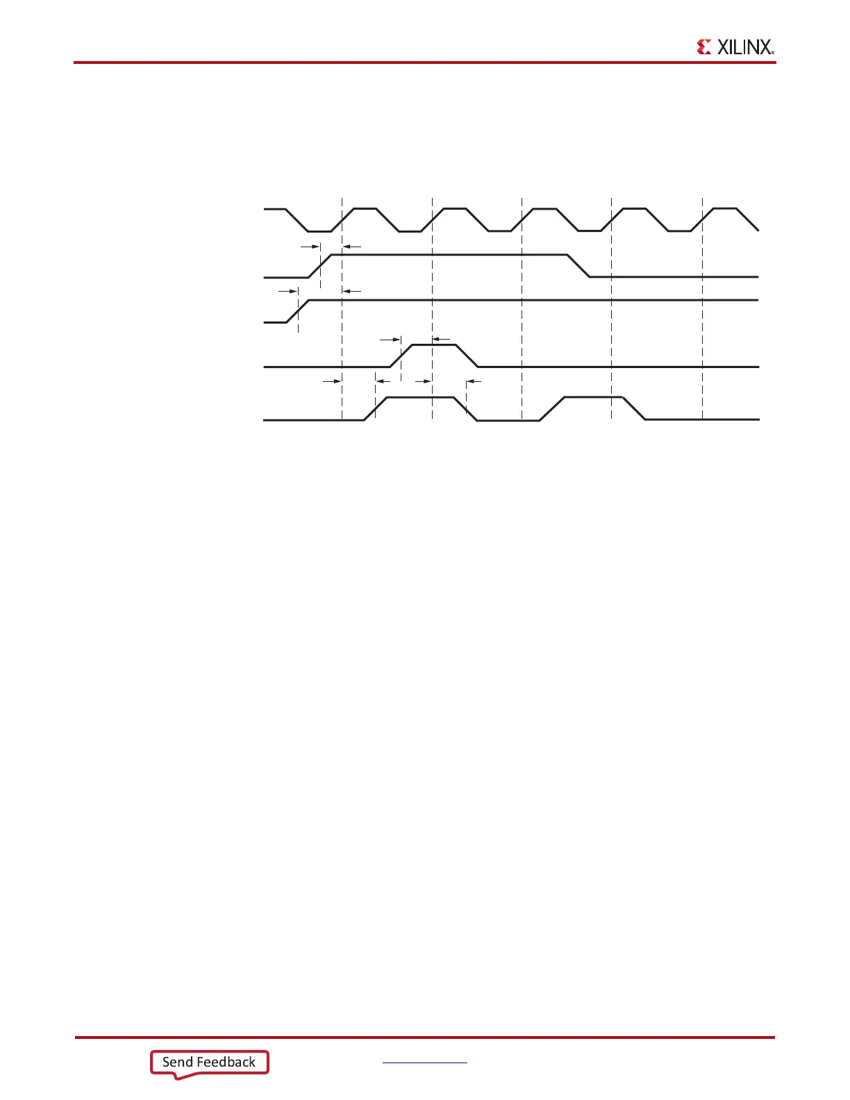
Figure 2-23 illustrates the OLOGIC 3-state register timing.
Clock Event 1
• At time T
OTCECK
before Clock Event 1, the 3-state clock enable signal becomes
valid-high at the TCE input of the 3-state register, enabling the 3-state register for
incoming data.
• At time T
OTCK
before Clock Event 1 the 3-state signal becomes valid-high at the T
input of the 3-state register, returning the pad to high-impedance at time T
OCKQ
after
Clock Event 1.
Clock Event 2
•At time T
OSRCK
before Clock Event 2, the S/R signal (configured as synchronous reset
in this case) becomes valid-high, resetting the 3-state register at time T
RQ
after Clock
Event 2.
X-Ref Target - Figure 2-2 3
Figure 2-23: OLOGIC 3-State Register Timing Characteristics
12345
CLK
T1
TCE
S/R
TQ
T
OCKQ
T
RQ
T
OTCK
T
OTCECK
T
OSRCK
UG471_c2_21_081215
 Loading...

