17-34
IM 05P02C41-01EN
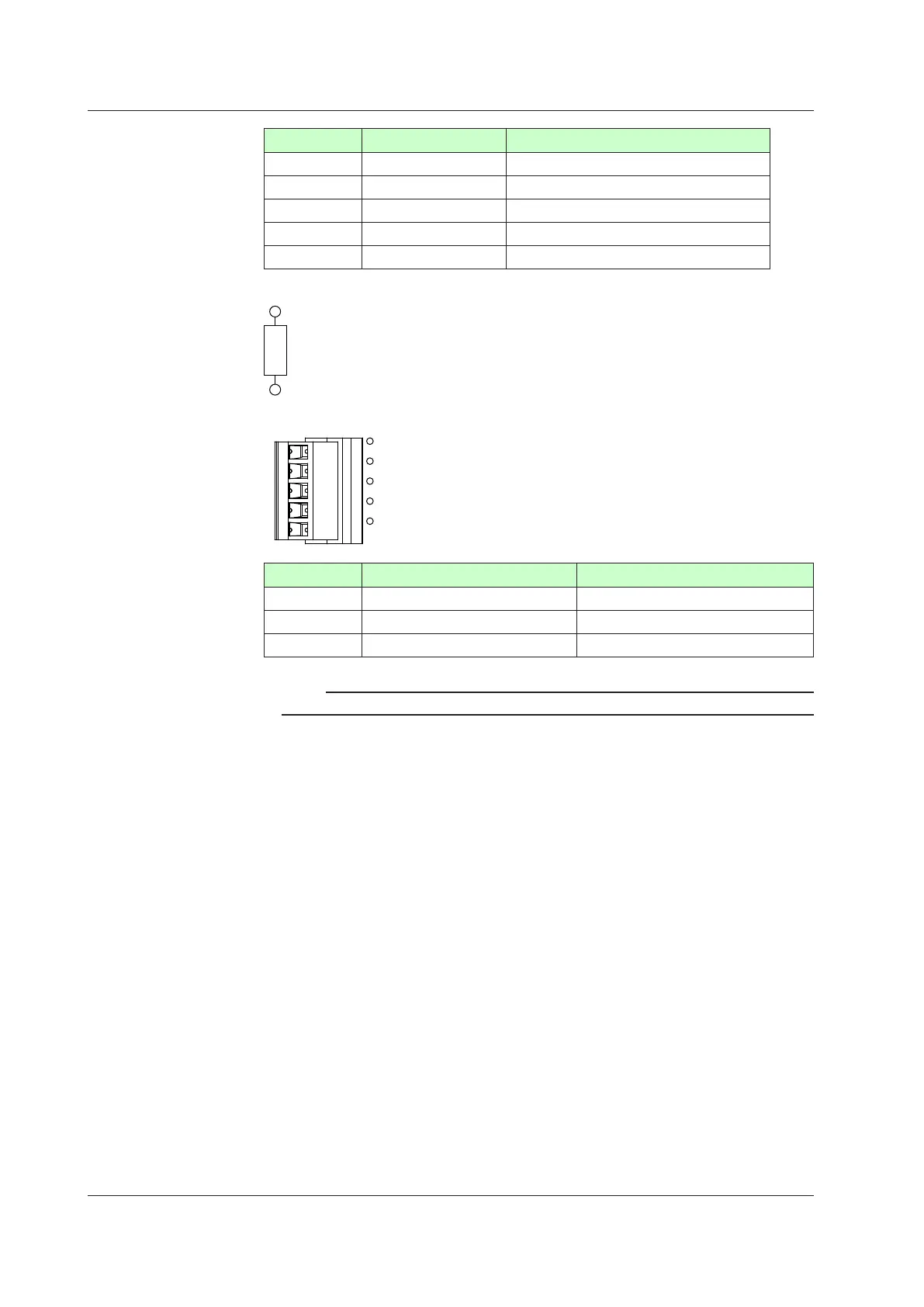
NumberofPin Singnalname Description
1 FG Frame ground
2 SLD Shield
3 DG TX/RXsignalground
4 DB RX/TX-signal
5 DA RS/TX+signal
TerminatingResisterofBus(bothendsofthetrunkline)
110Ω
CC-LinkcommunicationconnectorandLED
CHK
L ERR
LED Lit Unlit
CHK (red) Userproleerror/addresserror Normal
L ERR (red) Communication failure (CRC error) Normal
L RUN (green) Normal. Communicating successfully. No carrier detected. / Connection timeout.
Note
Use FG as an exclusive ground. Be sure to ground using a low grounding resistance.
Modbusmasterwiring
Modbus master wiring is same as RS-485 communication wiring for Ethernet-serial
gateway function.
17.4Wiring

 Loading...