12
All Rights Reserved. Copyright © 2010, Yokogawa Electric Corporation
GS 05P02C41-01EN Mar.14,2016-00
E3-Terminal Area
401-412
E4-Terminal Area
501-506
(Suffix code: Type 3=2,
except Type 2=3)
Ethernet communication (with gateway function)
10BASE-T/100BASE-TX
RJ45 connector
Color
Lit
Unlit
Amber
100M bps
10M bps
Green
Linked
Active
Link failure
Color
Lit
Blink
Unlit
Upper side LED (baud rate)
Lower side LED (link activity)
RS-485
RSB(+)
RSA(-)
SG
407
408
409
ETHR
RS-485
SDB(+)
SDA(-)
RDB(+)
RDA(-)
SG
RS-485 communication
(Suffix code: Type 3=1,
except Type 2=3)
407
408
409
410
411
RS485
Contact input
External contact input
DI41
DI42
DI43
DI44
DI45
COM
DI41
DI42
COM
+5V
+5V
DI43
+5V
DI44
+5V
DI45
+5V
UP UP
(Equipped as standard, however suffix code: Type 2= except 2 and 4)
Common
No-voltage contact
Transistor contact
Contact rating: 12 V DC, 10 mA or more
Bit-0 of
program pattern number
Bit-1 of
program pattern number
Bit-2 of
program pattern number
Bit-3 of
program pattern number
Bit-4 of
program pattern number
501
502
503
504
505
506
501
502
503
504
505
506
Function can be changed.
DI
Contact output
External contact output
DO32
DO31
DO33
DO34
DO35
COM
Time event-6 output
Time event-7 output
Time event-8 output
Time event-9 output
Time event-10 output
Common
UP
(Suffix code: Type 2=3)
407
408
409
410
411
412
DO
Transistor contact rating: 24 V DC, 50 mA
Function can be
assigned to the
terminals with no
function.
RS-485
SDB(+)
SDA(-)
RDB(+)
RDA(-)
SG
RS-485 communication
501
502
503
504
505
RS485
(Suffix code: Type 2=2)
Aux. analog input
Default: 1-5 V DC
+
-
Aux. analog input/Contact input
External contact input
DI46
COM
DI46
COM
+5V
UP UP
(Suffix code: Type 2=4)
Common
No-voltage contact
Transistor contact
Contact rating: 12 V DC, 10 mA or more
Factory default: No function
503
504
503
504
505
506
Function can be assigned to the
terminals with no function.
AIN4
Specify within a
range of 1-5 V DC,
0-2 V DC,0-10 V DC
A program pattern is selected with the combination of ON and OFF of a contact
input.
In the case of a pattern 5, ON (1) of "DI45 to DI41" and OFF (0) is represented
as a binary number "00101": it is "5" decimally.
The pattern 13 or later can be selected similarly.
Program pattern number
1 2 3 4 5 6 7 8 9 10 11 12
DI41 ON OFF ON OFF ON OFF ON OFF ON OFF ON OFF
DI42 OFF ON ON OFF OFF ON ON OFF OFF ON ON OFF
DI43 OFF OFF OFF ON ON ON ON OFF OFF OFF OFF ON
DI44 OFF OFF OFF OFF OFF OFF OFF ON ON ON ON ON
DI45 OFF OFF OFF OFF OFF OFF OFF OFF OFF OFF OFF OFF
(Suffix code: Type 3=5,
except Type 2=3)
DeviceNet communication (with Modbus master)
RS-485
RSB(+)
RSA(-)
SG
407
408
409
DNET
If the UP is located at the
end of a segment for the
DeviceNet
communication wiring,
terminating resistors are
separately needed.
These are to be
prepared by users. (121
Ω: 1 pc.)
CAN_H
CAN_L
121Ω
LED
CHK
(red)
MNS
(green/
red)
Lit/flashing
Unlit
User profile error
Normal
Pin
1
2
Signal name Description
CAN_H
CAN_L
3
V+
4
V-5
DRAIN
RX/TX + signal
RX/TX - signal
Shield/Drain wire
DeviceNet power supply 24V
DeviceNet power supply common
Normal. Communicating
successfully (green, lit).
Not connected (green, flashing).
Critical link failure (red, lit).
Communication timeout (red,
flashing)
At power-on/Communication
faulted (green/red, flashing)
No electricity
CHK
MNS
1
2
3
4
5
(Suffix code: Type 3=3,
except Type 2=3)
CC-Link communication (with Modbus master)
RS-485
RSB(+)
RSA(-)
SG
407
408
409
CC-L
If the UP is located at
the end of a segment
for the CC-Link
communication wiring,
terminating resistors
are separately needed.
These are to be
prepared by users.
(110 Ω: 1 pc.)
DA
DB
110Ω
LED
CHK
(red)
L ERR
(red)
L RUN
(green)
Lit
Unlit
Normal
Normal
Pin
1
2
Signal name Description
DA
DB
3 DG
4
SLD
5
FG
RX/TX + signal
RX/TX - signal
Frame ground
RX/TX signal ground
Shield
Normal
Communicating successfully
Communication failure (CRC
error)
No carrier
detected /
Connection
timeout
CHK
L RUN
L ERR
1
2
3
4
5
PROFIBUS-DP communication (with Modbus master)
Pin
1
2
Signal name Description
VP
RxD/TxD-P
3 RxD/TxD-N
4 DGND
5 SHIELD
+5V bus power
Data signal
(positive data receive/transmit)
Data signal
(negative data recive/transmit)
Signal ground
Shield ground
RS-485
RSB(+)
RSA(-)
SG
407
408
409
PROF
If the UP is located at the end
of a segment for the
PROFIBUS
communication wiring,
terminating resistors are
separately needed.
These are to be prepared by
users. (390 Ω: 2 pcs. 220 Ω: 1
pc., or an active
terminator.)
VP
RxD/TxD-P
Data
line
Data
line
390Ω
220Ω
390Ω
RxD/TxD-N
DGND
LED
CHK
(red)
RDY
(green)
Lit Unlit
ERR
(red)
User profile error Normal
Normal
Not connected, or
communication
failure (flashing)
Normal
Communicating
successfully
No electricity, or
Communication
failure
(Suffix code: Type 3=4,
except Type 2=3)
CHK
RDY
ERR
1
2
3
4
5
User profile error / Address
error
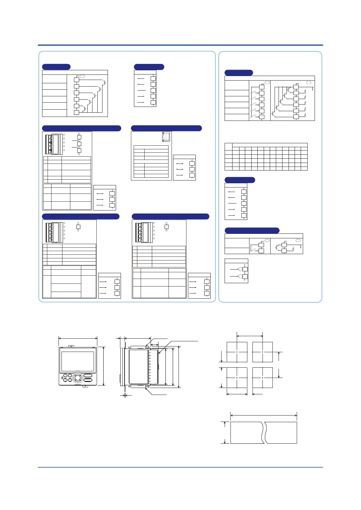
nExternalDimensionsandPanelCutoutDimensions
(25)
(53) (2.09)
[(N-1)×96+92]
117 (4.61) min.
145 (5.71)
min.
+0.8
0
+0.8
0
92
“N” stands for the number of controllers to be installed.
However, the measured value applies if N≥5.
65 (2.56)
20 (0.79)
11
(0.43)
1 to 10 mm (0.04 to 0.39 inch) (panel thickness)
Bracket
Bracket
94.6 (3.72)
91.6 (3.61)
105.2 (4.14)
Unit: mm (approx. inch)
96 (3.78)
96 (3.78)
• Side-by-side close mounting
Terminal cover
Normal tolerance:
±(value of JIS B 0401-1998 tolerance class IT18)/2
+0.8
0
92
+0.03
0
(3.62 )
(0.98)
+0.03
0
(3.62 )
+0.8
0
92
+0.03
0
(3.62 )
([(N-1)×3.78+3.62] )
+0.03
0

 Loading...