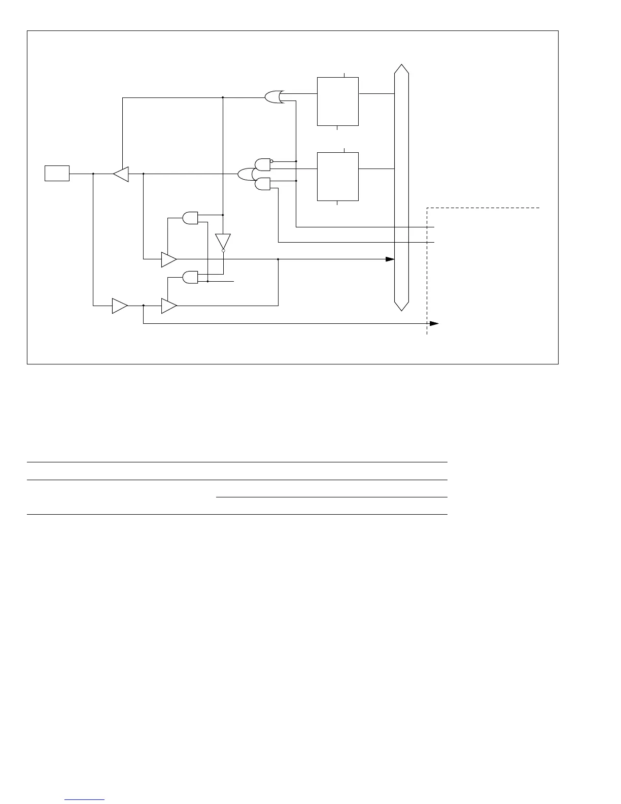
Table C-7 (d) Port 7 Port Read (Pins P74 – P76)
Setting Port Read Data
Output enable Output compare output value
DDR = 0 Pin value
DDR = 1 DR value
RP7
P7
n
WP7
Free-running timer module
Output enable
Output compare output
WP7D:
WP7:
RP7:
n:
Write to P7DDR
Write to Port 7
Read Port 7
4, 5 or 6
Internal data bus (PDB12 to PDB14)
C
R
QD
P7 DR
n
C
R
QD
P7 DDR
n
Reset
Reset
WP7D
Counter clock output
Output disable
Figure C-7 (d) Schematic Diagram of Port 7, Pins P74, P75 and P76
421
Downloaded from Elcodis.com electronic components distributor

 Loading...
