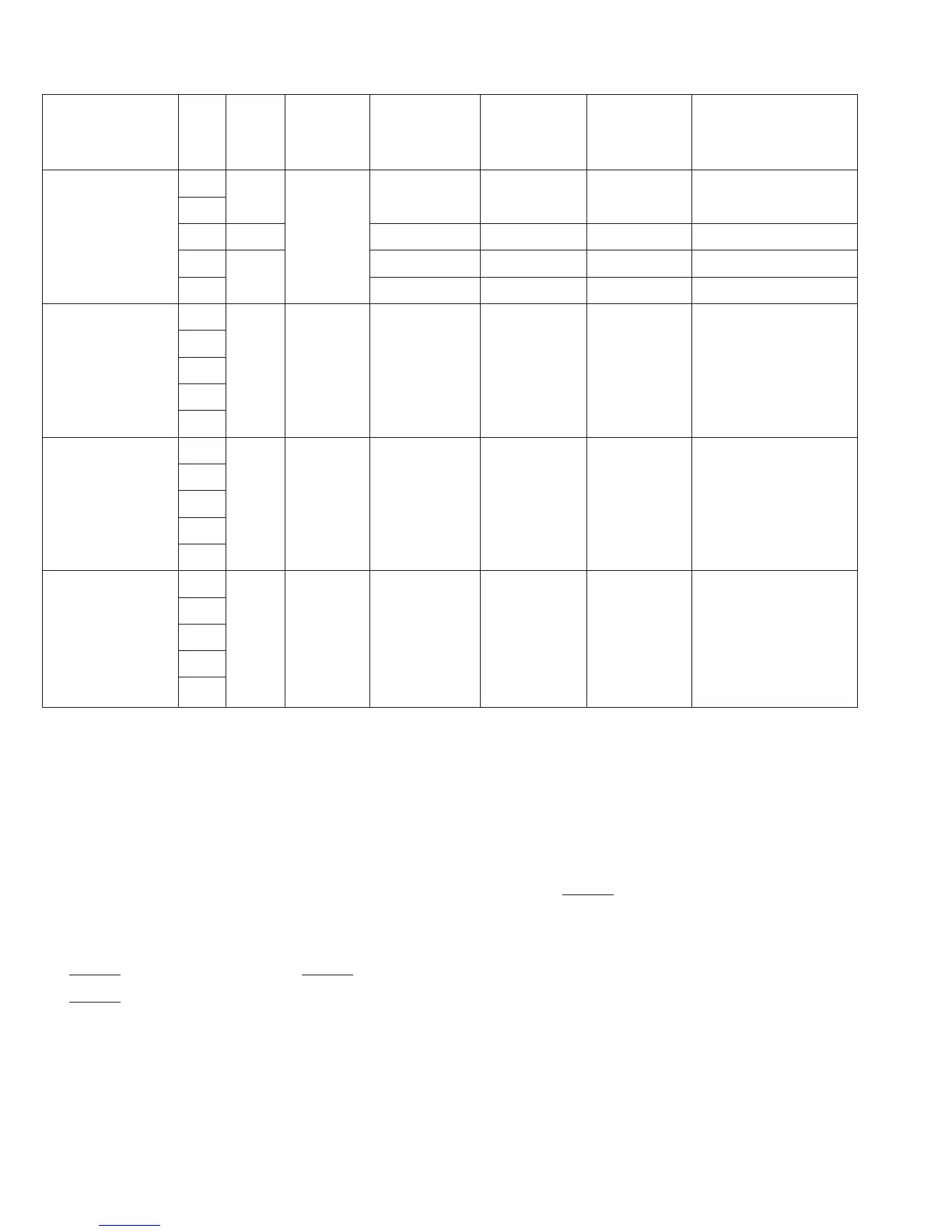
Table E-1 Port State (cont)
Hardware
Port Standby Software Bus-right Program Execution
Pin Name Mode Reset Mode Standby mode Sleep Mode Release Mode
State (Normal Operation)
P63 to P60 1
A19 to A16 2T
3L T T L T A19 to A16
4T T
*
6
*
5
T
*
6
Address/Input port
7 keep keep --- Input/Output port
P77 to P70 1
2
3 T T keep
*
2
keep keep Input port
4
7
P87 to P80 1
2
3 T T T T T Input port
4
7
P97 to P90 1
2
3 T T keep
*
2
keep keep Input/Output port
4
7
H: “High” = High level
L: “Low” = Low level
T: High Impedance
keep: If DDR = 0 and DR = 1 in port 5 and 6, Pull-up MOS holds on-state.
Notes:
*1 8 Bit Timer is reset, so P1
7 becomes input or output port controlled by DDR and DR. Also P12
goes to the high impedance state when it is programmed as BACK output.
*2 On-chip supporting modules are reset. So these pins become input or output ports controlled
by DDR and DR.
*3 BREQ can be accepted and BACK goes LOW.
*4 BACK outputs LOW.
*5 The pins programmed as address bus output LOW and others programmed as input are at the
high impedance state.
If DDR = 0 and DR = 1, the pull-up MOS’s keep ON state.
*6 If DDR = 0 and DR = 1, the pull-up MOS’s keep ON state.
keep keep keep Input/Output port
432
Downloaded from Elcodis.com electronic components distributor

 Loading...
