Because RFL™ and Hubbell® have a policy of continuous product improvement, we reserve the right to change designs and specifications without notice.
Table 6. Connector J1 pin assignments for the MA-410I Module adapter
Pin No. Signal Name
1 Chassis
2 TX Data A
3 Control A
4 Rx Data A
5 Indicate A
6 Signal Timing A
8 Signal Ground
9 Tx Data B
10 Control B
11 Rx Data B
12 Indicate B
13 Signal Timing B
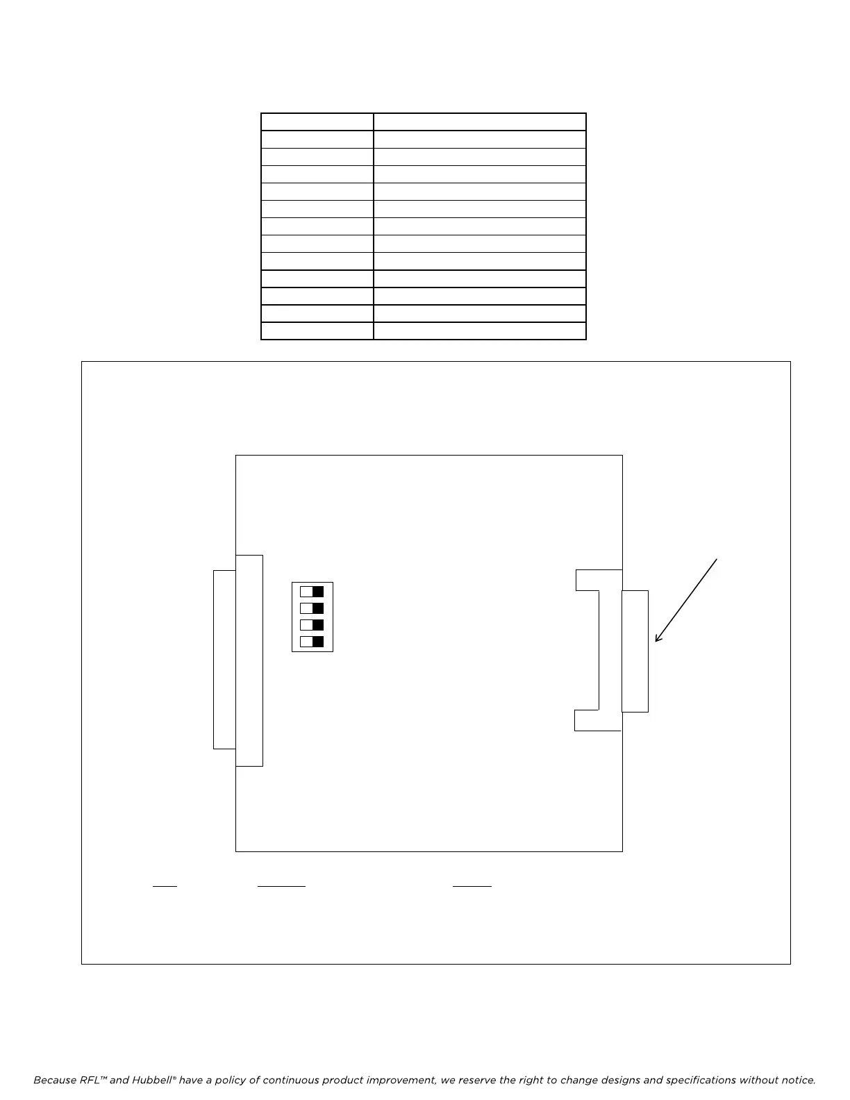
Item Function Setting
DIP Switch S1 Selects DCE or DTE mode DCE: S1-1 to S1-4 toward “DCE”
DTE: S1-1 to S1-4 toward “DTE”
Item
Function Setting
R2 Receive data/timing (factory adjustment)
output level adjust
Connector J1
(See Table 6
for pin assign-
mens)
S1
DTE DCE
Figure 6. Controls and Indicators, MA-410I Module adapter
RFL DS-562I RFL El
ectronics Inc.
June 14, 2007 13 (973)
334-3100