Because RFL™ and Hubbell® have a policy of continuous product improvement, we reserve the right to change designs and specifications without notice.
Table 5. Connector J1 pin assignments for the MA-409IA Module Adapter
V.35 Pin No. Signal Name DC-37S Pin No.
S SD (B) - Send Data 22
P SD (A) - Send Data 4
AA SCT (B) - Serial Clock Transmit 23
Y SCT (A) - Serial Clock Transmit 5
X SCR (B) - Serial Clock Receive 26
V SCR (A) - Serial Clock Receive 8
T RD (B) - Receive Data 24
R RD (A) - Receive Data 6
D CB - Clear To Send (CTS) 9
C CA - Request To Send (RTS) 7
B AB - Signal Ground 19
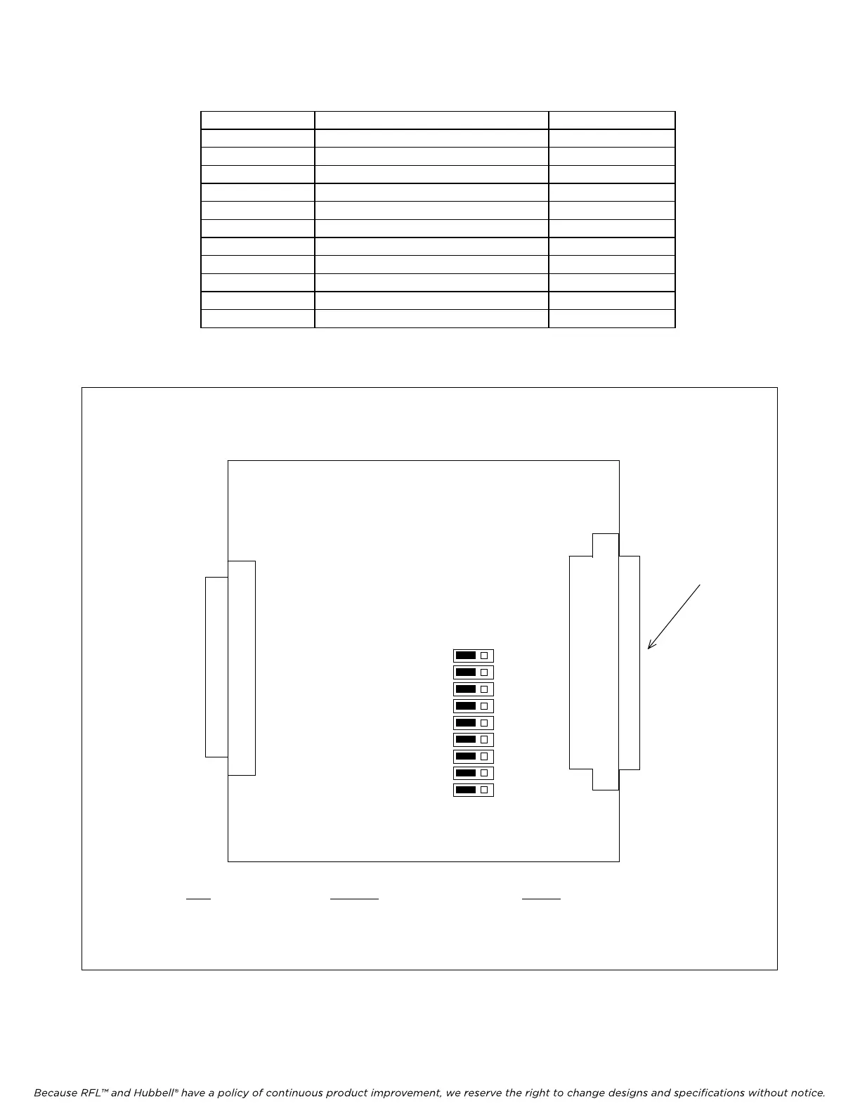
Item Function Setting
Jumpers J1 to J9 Select DCE or DTE mode
DCE: Set all jumpers to DCE
DTE: Set all jumpers to DTE
Connector J1
(See Table 5
for pin assign-
ments)
DCE DTE
J1
J2
J3
J4
J5
J6
J7
J8
J9
Figure 5. Controls and indicators, MA-409IA Module Adapter
RFL DS-562I RFL E
lectronics Inc.
June 14, 2007 12 (973) 334-3100