Because RFL™ and Hubbell® have a policy of continuous product improvement, we reserve the right to change designs and specifications without notice.
Table 4. Connector J1 pin assignments for the MA-408I Module Adapter
Pin No. Signal Name
1 GND - Chassis
2 TD(A) - Transmit Data (input)
9 TD(B) - Transmit Data (input)
3 RD(A) - Receive Data (output)
16 RD(B) - Receive Data (output)
Note: The clock is embedded within the Transmit and Receive data signal.
The customer interface recovers the clock provided by the MA-408I
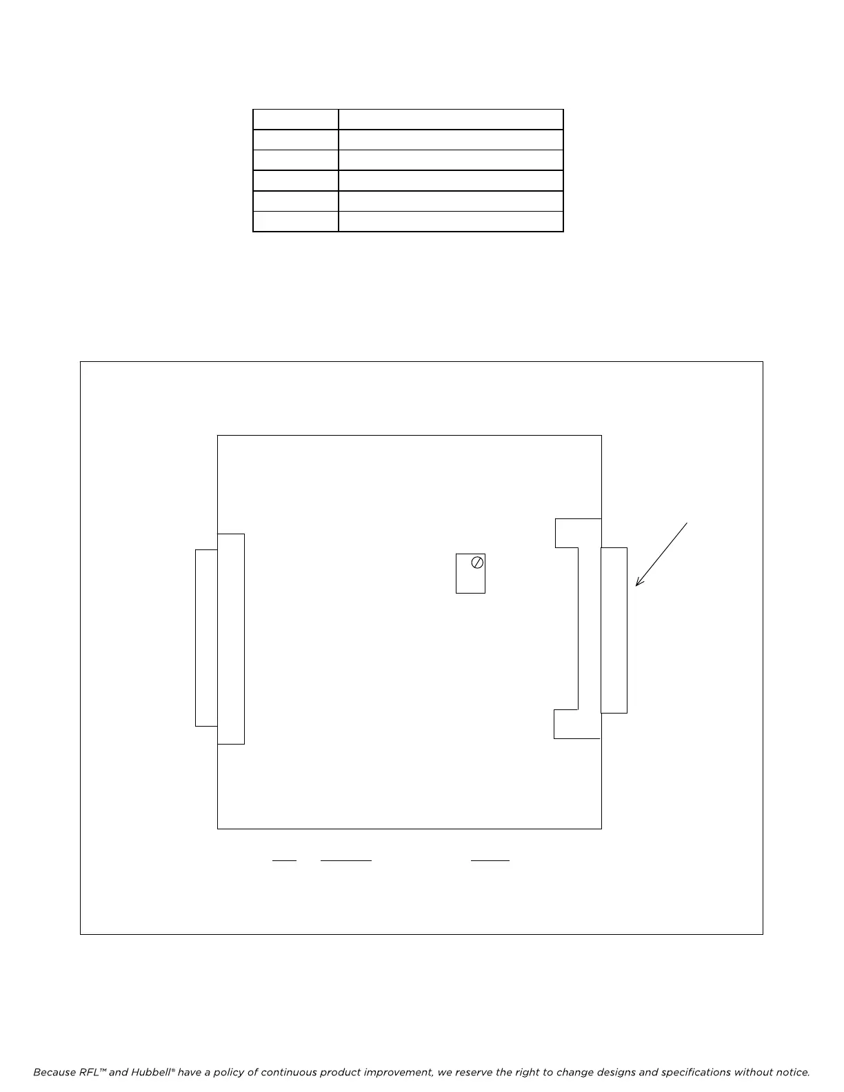
Item Function Setting
R2 Receive data/timing (factory adjustment)
output level adjust
Connector J1
(See Table 4
for pin assign-
ments)
R2
Figure 4. Controls and indicators, MA-408I Module Adapter
RFL DS-562I RFL El
ectronics Inc.
June 14, 2007 11 (973)
334-3100