Because RFL™ and Hubbell® have a policy of continuous product improvement, we reserve the right to change designs and specifications without notice.
RFL OCUDP RFL Electronics Inc.
July 15, 2010 7 (973) 334-3100
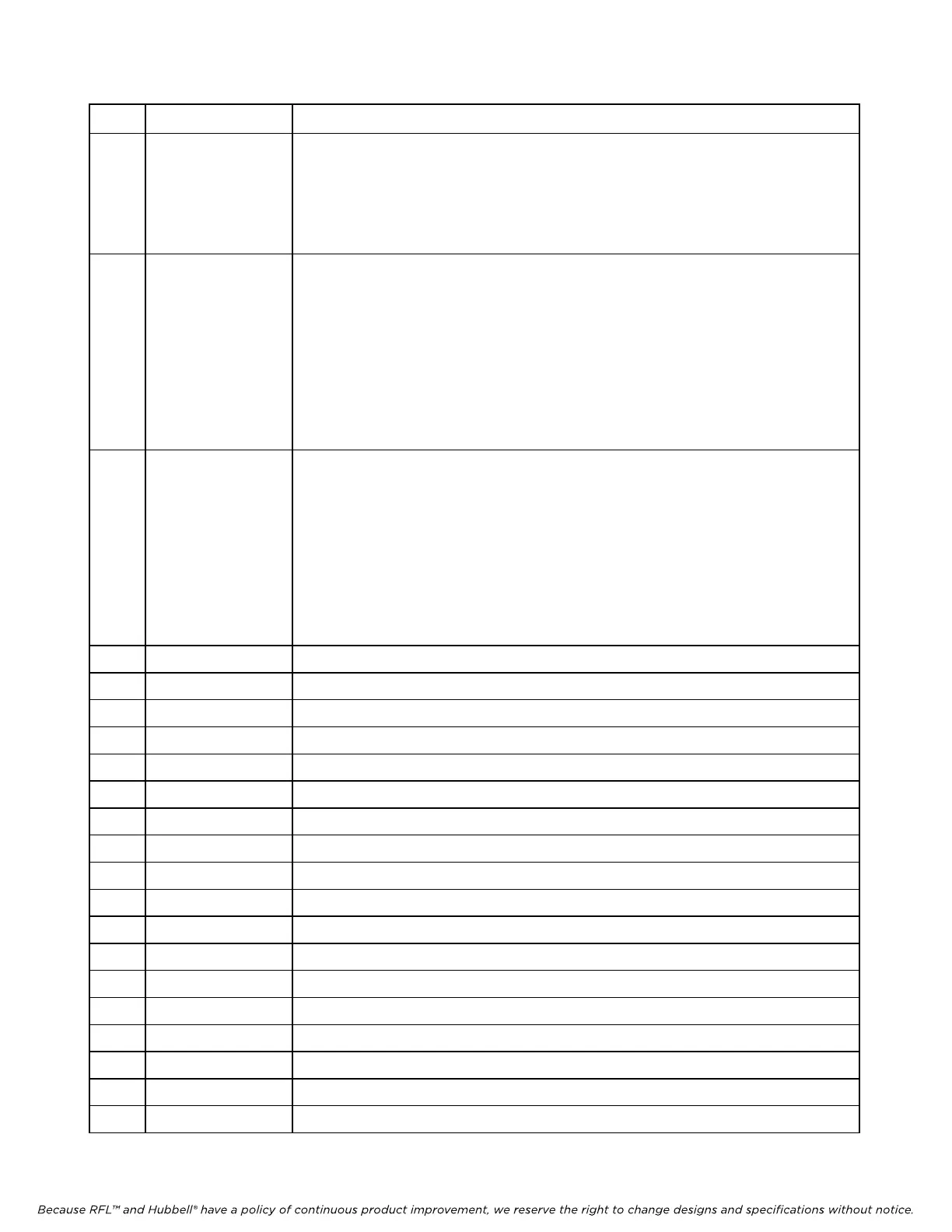
Table 1 - continued. Controls and indicators, RFL OCUDP Module
Item Name/Description Function
11 DIP Switch, SW2 SW2-1 to SW2-5 Sets Transmit Channel timeslot (See Table 3)
SW2-6 Module Service ON/OFF switch. SW2-6 in the ON/RIGHT position turns
Service OFF.
SW2-6 in the OFF/LEFT position turns Service ON.
SW2-7 to SW2-8 Not used.
12 DIP Switch, SW3 SW3-1 to SW3-5 Sets Receive Channel timeslot (See Table 3)
SW3-6 Sets the transmit bus direction. Set to OFF/LEFT to transmit in direction A
and receive from direction B (default). Set to ON/RIGHT to transmit in
direction B and receive from direction A.
When the OCUDP Module is in a terminal-end multiplexer, the OCUDP
Mod
ule must be configured to transmit in direction A.
SW3-7 Not used.
SW3-8 Alert on loss of Sealant Current. To enable set to OFF/LEFT.
To disable set to ON/RIGHT (default)
13 DIP Switch, SW4 SW4-1 to SW4-4 Sets baud rate (See Table 4)
SW4-5 Switched – 56k mode – not supported, must be set to ON/RIGHT for normal
mode.
SW4-6 ZCS (zero code suppression). Set to OFF/LEFT to enable,
Set to ON/RIGHT to disable.
S
W4-7 AB signaling enable. Set to OFF/LEFT to enable, set to ON/RIGHT to
disable.
SW4-8 Latched loopback Functionality
. Set to OFF?
LEFT to enable,
Set to ON/RIGHT to disable.
14 J5 Bantam Test Jacks (J5-A Input, J5-B Output)
15 Test Point TP13 TX- Negative side of transmitted bipolar signal
16 Test Point TP12 TX+ Positive side of transmitted bipolar signal
17 Test Point TP10 RX+ Positive side of received bipolar signal
18 Test Point TP11 RX- Negative side of received bipolar signal
19 Test Point TP6 TCLK Timing clock for transmitted logic signals
20 Test Point TP7 RPOS Logic signal from received bipolar positive pulse
21 Test Point TP8 RNEG Logic signal from received bipolar negative pulse
22 Test Point TP9 RCLK Timing clock for received logic signals
23 Test Point TP4 TPOS Logic input which generates positive pulse of bipolar output signal
24 Test Point TP5 TNEG Logic input which generates negative pulse of bipolar output signal
25 Test Point TP3 FRAME Frame pulse
26 Test Point TP2 ADDR OK Channel address pulse
27 Test Point TP1 Ground Signal ground
28 J3 ACTEL connector Used for factory testing
29 J4 ACTEL connector Used for factory testing
30 J2 Test/Run jumper Set to RUN position
31 J1 Serial port Used for factory testing
 Loading...