AES hardware accelerator (AES) RM0453
680/1454 RM0453 Rev 2
Note: The data in AES key registers (AES_KEYRx) and initialization registers (AES_IVRx) are not
sensitive to the swap mode selection.
Data padding
Figure 124 also gives an example of memory data block padding with zeros such that the
zeroed bits after the data swap form a contiguous zone at the MSB end of the AES core
input buffer. The example shows the padding of an input data block containing:
• 48 message bits, with DATATYPE[1:0] = 01
• 56 message bits, with DATATYPE[1:0] = 10
• 34 message bits, with DATATYPE[1:0] = 11
23.4.14 AES key registers
The AES_KEYRx write-only registers store the encryption or decryption key bitfield
KEY[127:0] or KEY[255:0]. The data to write to each register is organized in the memory in
little-endian order, that is, with most significant byte on the highest address (reads are not
allowed for security reason).
The key is spread over eight registers as shown in Table 138.
The key for encryption or decryption may be written into these registers when the AES
peripheral is disabled, by clearing the EN bit of the AES_CR register.
The key registers are not affected by the data swapping controlled by DATATYPE[1:0]
bitfield of the AES_CR register.
23.4.15 AES initialization vector registers
The four AES_IVRx registers keep the initialization vector input bitfield IVI[127:0]. The data
to write to or to read from each register is organized in the memory in little-endian order, that
is, with most significant byte on the highest address. The registers are also ordered from
lowest address (AES_IVR0) to highest address (AES_IVR3).
The signification of data in the bitfield depends on the chaining mode selected. When used,
the bitfield is updated upon each computation cycle of the AES core.
Write operations to the AES_IVRx registers when the AES peripheral is enabled have no
effect to the register contents. For modifying the contents of the AES_IVRx registers, the EN
bit of the AES_CR register must first be cleared.
Reading the AES_IVRx registers returns the latest counter value (useful for managing
suspend mode).
The AES_IVRx registers are not affected by the data swapping feature controlled by the
DATATYPE[1:0] bitfield of the AES_CR register.
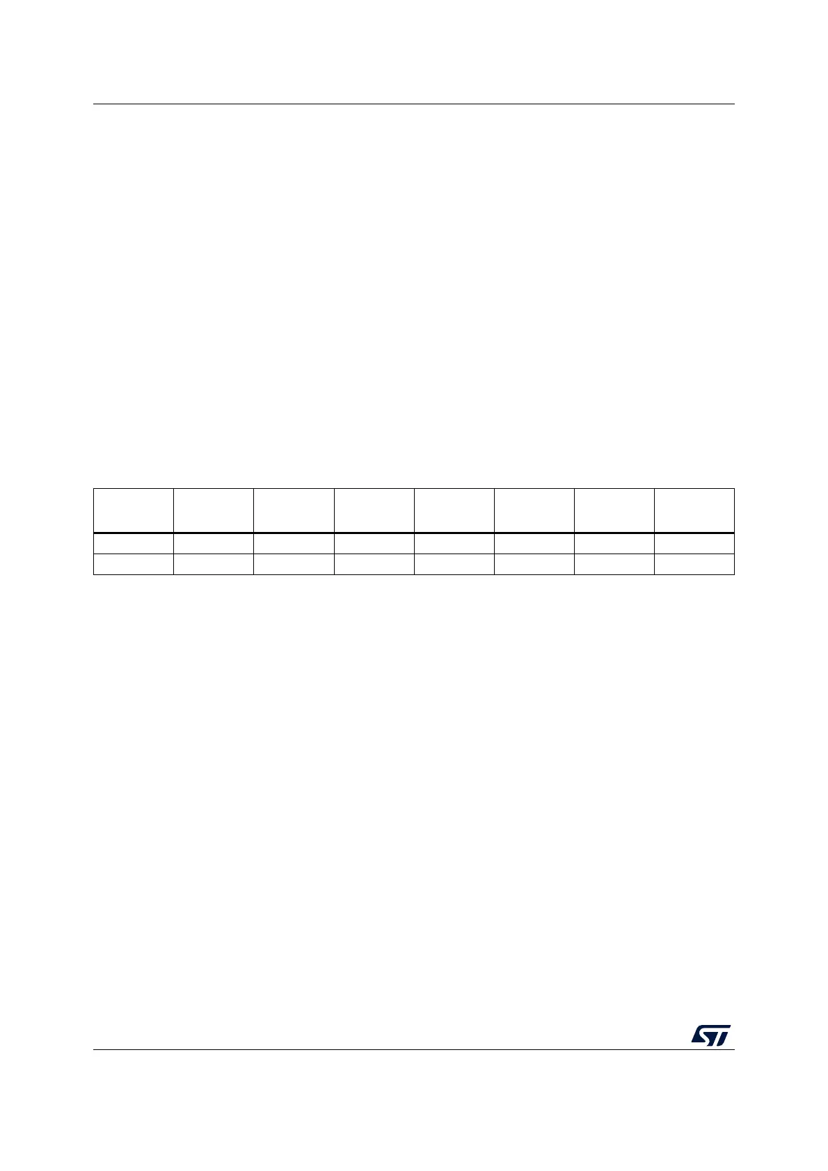
Table 138. Key endianness in AES_KEYRx registers (128- or 256-bit key length)
AES_KEYR7
[31:0]
AES_KEYR6
[31:0]
AES_KEYR5
[31:0]
AES_KEYR4
[31:0]
AES_KEYR3
[31:0]
AES_KEYR2
[31:0]
AES_KEYR1
[31:0]
AES_KEYR0
[31:0]
- - - - KEY[127:96] KEY[95:64] KEY[63:32] KEY[31:0]
KEY[255:224] KEY[223:192] KEY[191:160] KEY[159:128] KEY[127:96] KEY[95:64] KEY[63:32] KEY[31:0]

 Loading...


