General-purpose timer (TIM2) RM0453
888/1454 RM0453 Rev 2
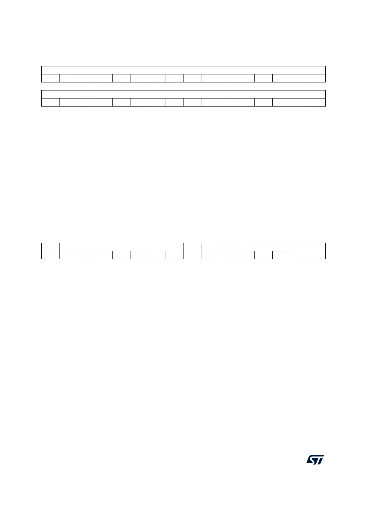
26.4.20 TIM2 DMA control register (TIM2_DCR)
Address offset: 0x48
Reset value: 0x0000
31 30 29 28 27 26 25 24 23 22 21 20 19 18 17 16
CCR4[31:16]
rw rw rw rw rw rw rw rw rw rw rw rw rw rw rw rw
1514131211109876543210
CCR4[15:0]
rw rw rw rw rw rw rw rw rw rw rw rw rw rw rw rw
Bits 31:0 CCR4[31:0]: Capture/Compare value
1. if CC4 channel is configured as output (CC4S bits):
CCR4 is the value to be loaded in the actual capture/compare 4 register (preload value).
It is loaded permanently if the preload feature is not selected in the TIMx_CCMR2
register (bit OC4PE). Else the preload value is copied in the active capture/compare 4
register when an update event occurs.
The active capture/compare register contains the value to be compared to the counter
TIMx_CNT and signalled on OC4 output.
2. if CC4 channel is configured as input (CC4S bits in TIMx_CCMR4 register):
CCR4 is the counter value transferred by the last input capture 4 event (IC4). The
TIMx_CCR4 register is read-only and cannot be programmed.
1514131211109876543210
Res. Res. Res. DBL[4:0] Res. Res. Res. DBA[4:0]
rw rw rw rw rw rw rw rw rw rw
Bits 15:13 Reserved, must be kept at reset value.
Bits 12:8 DBL[4:0]: DMA burst length
This 5-bit vector defines the number of DMA transfers (the timer recognizes a burst transfer
when a read or a write access is done to the TIMx_DMAR address).
00000: 1 transfer,
00001: 2 transfers,
00010: 3 transfers,
...
10001: 18 transfers.
Bits 7:5 Reserved, must be kept at reset value.
Bits 4:0 DBA[4:0]: DMA base address
This 5-bit vector defines the base-address for DMA transfers (when read/write access are
done through the TIMx_DMAR address). DBA is defined as an offset starting from the
address of the TIMx_CR1 register.
Example:
00000: TIMx_CR1
00001: TIMx_CR2
00010: TIMx_SMCR
...
Example: Let us consider the following transfer: DBL = 7 transfers & DBA = TIMx_CR1. In
this case the transfer is done to/from 7 registers starting from the TIMx_CR1 address.

 Loading...


