100 www.xilinx.com 7 Series FPGAs SelectIO Resources User Guide
UG471 (v1.10) May 8, 2018
Chapter 1: SelectIO Resources
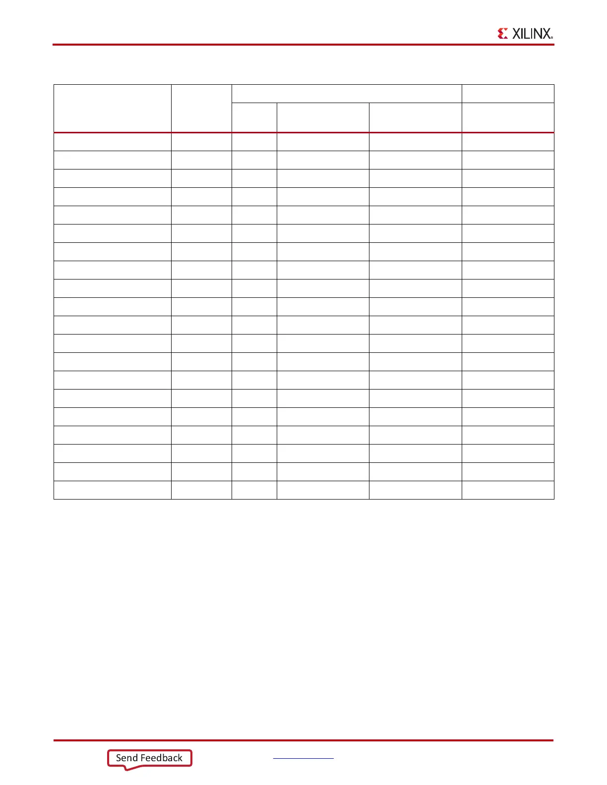
LVTTL HR 3.3 3.3 N/A N/A
MINI_LVDS_25 HR 2.5
(2)
2.5
(1)
2.5 N/A
MOBILE_DDR HR 1.8 1.8 N/A N/A
PCI33_3 HR 3.3 3.3 N/A N/A
PPDS_25 HR 2.5
(2)
2.5
(1)
2.5 N/A
RSDS_25 HR 2.5
(2)
2.5
(1)
2.5 N/A
SSTL135 Both 1.35 Any N/A 0.675
SSTL135_R HR 1.35 Any N/A 0.675
SSTL135_DCI HP 1.35 1.35 N/A 0.675
SSTL135_T_DCI HP 1.35 1.35 N/A 0.675
SSTL15 Both 1.5 Any N/A 0.75
SSTL15_R HR 1.5 Any N/A 0.75
SSTL15_DCI HP 1.5 1.5 N/A 0.75
SSTL15_T_DCI HP 1.5 1.5 N/A 0.75
SSTL18_I Both 1.8 Any N/A 0.9
SSTL18_I_DCI HP 1.8 1.8 N/A 0.9
SSTL18_II Both 1.8 Any N/A 0.9
SSTL18_II_DCI HP 1.8 1.8 N/A 0.9
SSTL18_II_T_DCI HP 1.8 1.8 N/A 0.9
TMDS_33 HR 3.3 Any N/A N/A
Notes:
1. Differential inputs for these standards can be placed in banks with V
CCO
levels that are different from the required level for
outputs. There are some important criteria that need to be considered:
a. The optional internal differential termination is not used (DIFF_TERM = FALSE, which is the default value) unless the V
CCO
voltage is at the level required for outputs.
b. The differential signals at the input pins meet the V
IN
requirements in the Recommended Operating Conditions table of the
specific device family data sheet.
c. The differential signals at the input pins meet the V
IDIFF
and V
ICM
requirements in the corresponding LVDS or LVDS_25 DC
Specifications tables in the specific device family data sheet. In some cases, to accomplish this it might be necessary to provide
an external circuit to both AC-couple and DC-bias the pins.
2. If the voltage exceeds 2.85V, the outputs will be in a high-Z state. The device should always be operated within the recommended
operating range as specified in the 7 series FPGA data sheets.
Table 1-55: V
CCO
and V
REF
Requirements for Each Supported I/O Standard (Cont’d)
I/O Standard
I/O Bank
Availability
V
CCO
(V) V
REF
(V)
Output Input
Input with
DIFF_TERM = TRUE
Input