GR712RC-UM, Jun 2017, Version 2.9 152 www.cobham.com/gaisler
GR712RC
18.6.3 Bus timing 1
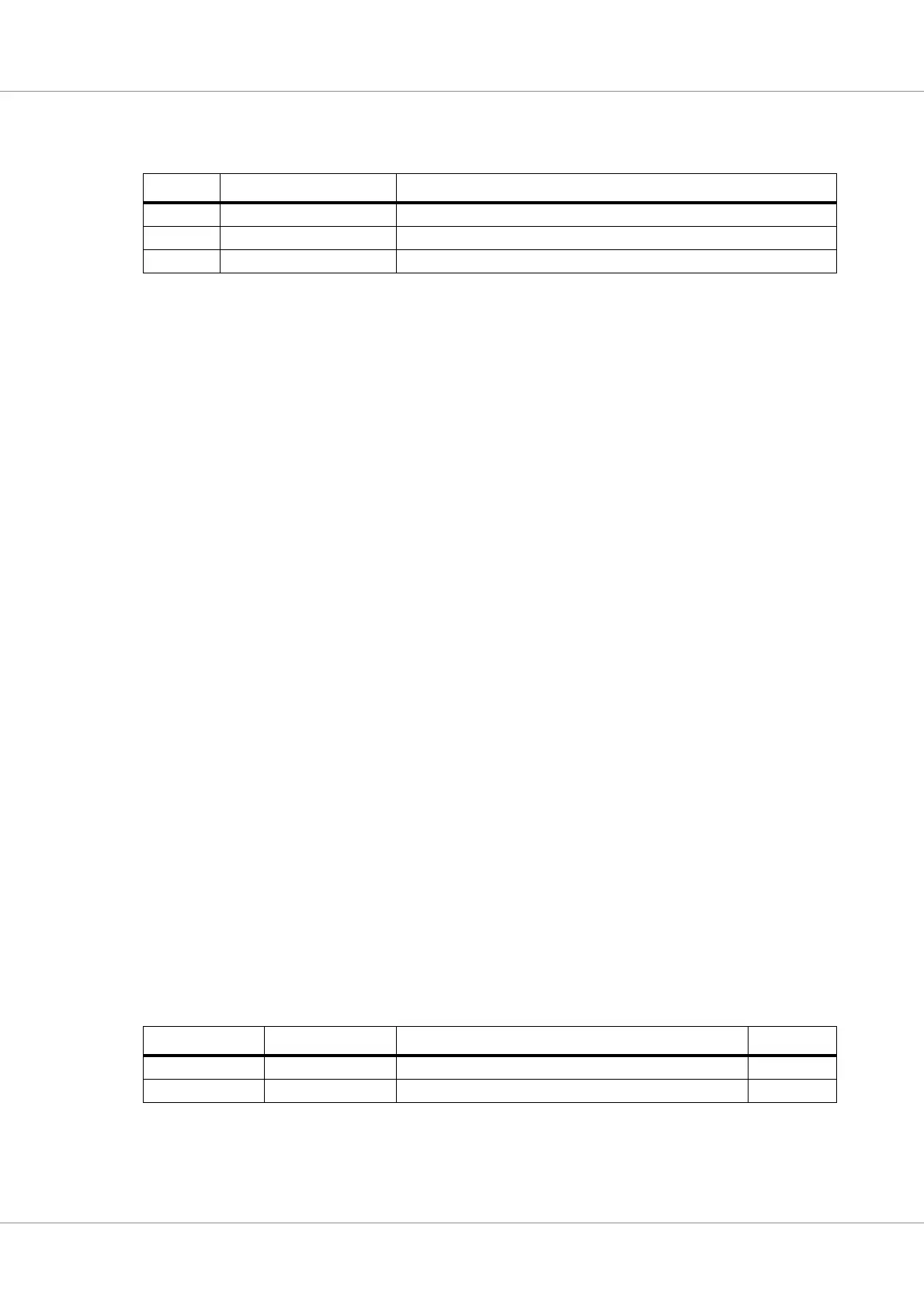
Table 154.Bit interpretation of bus timing 1 register (BTR1) (address 7)
The CAN bus bit period is determined by the CAN system clock and time segment 1 and 2 as shown
in the equations below:
t
tseg1
= t
scl
* (TSEG1+1)
t
tseg2
= t
scl
* (TSEG2+1)
t
bit
= t
tseg1
+ t
tseg2
+ t
scl
The additional t
scl
term comes from the initial sync segment. Sampling is done between TSEG1 and
TSEG2 in the bit period.
18.7 Design considerations
This section lists known differences between this CAN controller and SJA1000 on which is it based:
• All bits related to sleep mode are unavailable
• Output control and test registers do not exist (reads 0x00)
• Clock divisor register bit 6 (CBP) and 5 (RXINTEN) are not implemented
• Overrun irq and status not set until fifo is read out
BasicCAN specific differences:
• The receive irq bit is not reset on read, works like in PeliCAN mode
• Bit CR.6 always reads 0 and is not a flip flop with no effect as in SJA1000
PeliCAN specific differences:
• Writing 256 to tx error counter gives immediate bus-off when still in reset mode
• Read Buffer Start Address register does not exist
• Addresses above 31 are not implemented (i.e. the internal RAM/FIFO access)
• The core transmits active error frames in Listen only mode
18.8 Signal definitions
The signals are described in table 155.
Bit Name Description
BTR1.7 SAM 1 - The bus is sampled three times, 0 - single sample point
BTR1.6-4 TSEG2 Time segment 2
BTR1.3-0 TSEG1 Time segment 1
Table 155.Signal definitions
Signal name Type Function Active
CANTX[] Output CAN transmit data Low
CANRX[] Input CAN receive data Low