GR712RC-UM, Jun 2017, Version 2.9 172 www.cobham.com/gaisler
GR712RC
24 SLINK Serial Bus Based Real-Time Network Master
24.1 Overview
The core provides a link between the AMBA bus and the SLINK Serial Bus Based Real-Time Net-
work. The core is configured through registers mapped into AMBA APB address space and can also
perform DMA operations via AMBA AHB. A DMA engine enables it to perform sequences of
SLINK operations without CPU intervention. Single operations are performed via the register inter-
face. The core generates the SLINK SCLK clock and SYNC signals by dividing the system clock.
24.2 Operation
24.2.1 Transmission protocol
The SLINK bus is a full duplex synchronous bus that connects one master to seven slaves. The bus
contains four differential lines, data to the master (SDI), data from the master (SDO), a periodic syn-
chronization signal (SYNC) and a clock line (SCLK). The SCLK clock operates at 6 MHz continu-
ously, one cycle of this clock constitutes a SLINK bit time. Words sent on the SLINK bus are 25 bits
long and are always followed by a SYNC pulse that lasts one SLINK bit time, which results in a word
time of 26 SLINK bit times. The data word formats are shown in figures 182 and 183.
When the bus is inactive the master sends NULL messages, see figure 184, and listens to the SDI lines
for traffic from the slaves. The NULL word shown in figure 184 is the default word with odd parity,
the contents of the NULL word is configurable via the NULL word register and the core’s use of par-
ity is configurable via the Control register.
The SLINK specification defines four types of data transfers:
Table 181.SLINK data transfer types
Transfer type Description
MASTER-WORD-SEND The master sends one READ or WRITE command. In case of a
READ command a slave will respond in a later SYNC cycle.
INTERRUPT A slave sends a word where the channel # field is set to 0.
SLAVE-WORD-SEND An unsolicited word sent from a slave that is not an INTERRUPT
nor a response to a READ command.
SEQUENCE The master performs a sequence of operations described by an in-
memory array which has a maximum size of 1024 elements.
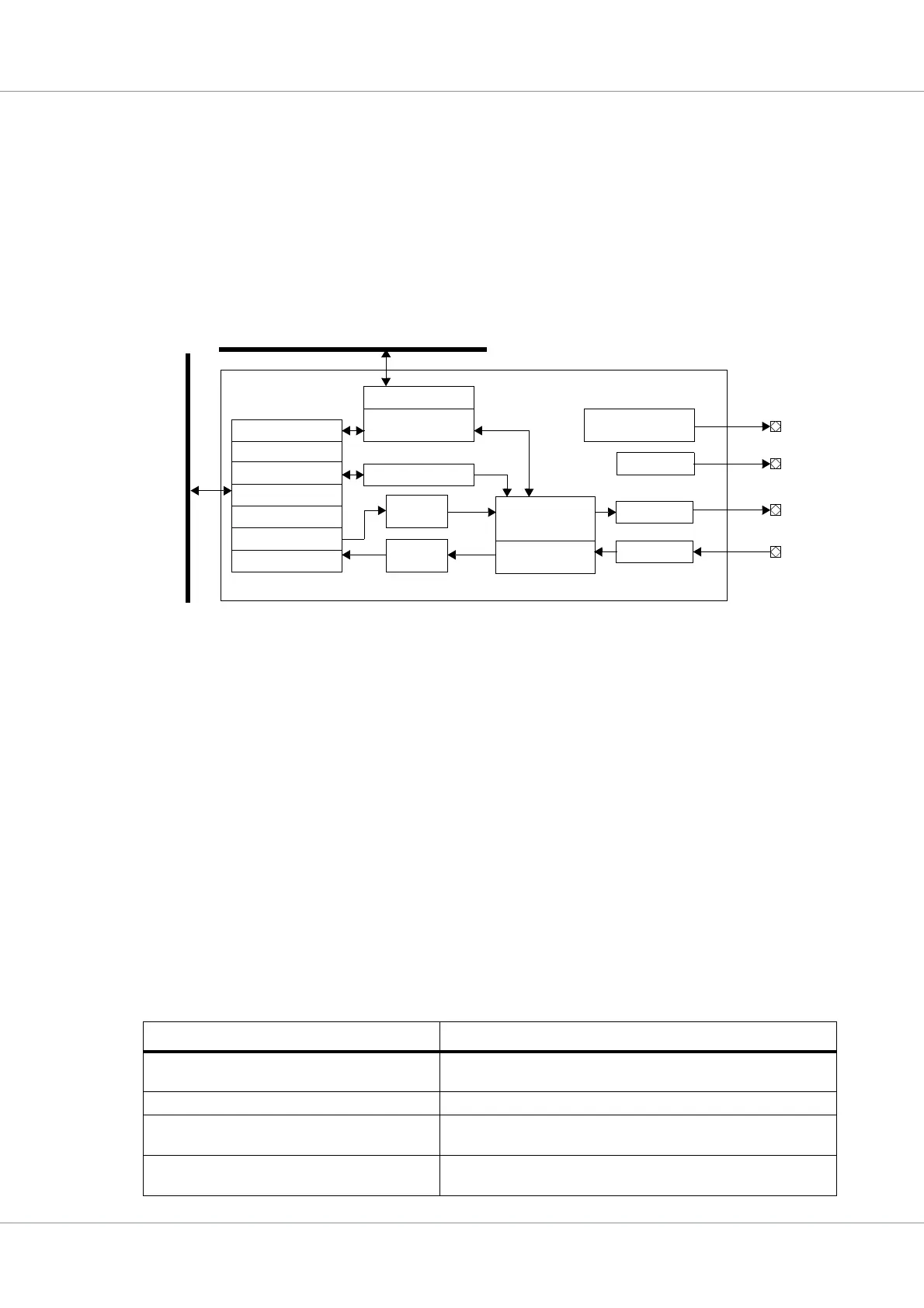
Figure 75. Block diagram
A
M
B
A
A
P
B
Transmit
Scale register
Status register
Mask register
Base registers
Transmit register
Receive register
FIFO
Receive
FIFO
SCLK
DMA engine
AMBA AHB
Control FSM
SYNC gen.
SYNC
Shift reg.
SDI
SDO
with FIFOs
Control register
Receive detection
Clock generator
Transmit
arbitration
AHB Master
Shift reg.